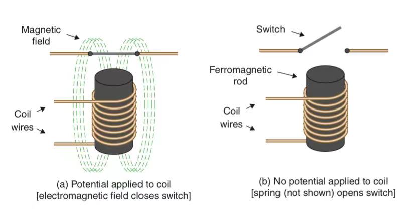
The Electromechanical Relay
- The relay consisted of a rod of iron wrapped in a coil of wire, applying an electrical potential across the ends of the coil caused the iron rod to act like a magnet. The magnetic field could be used to attract another iron acting as a switch.
- Connecting relays together in different ways makes it possible to create all sorts of functions because the outputs from one or more relays can be used to control other relays.
- The problem with relays is that they can only switch a limited number of times a second, it limits the performance of the computer.
Vacuum Tubes
- Edison’s assistant discovered that he could detect electrons flowing through the vacuum from the lighted filament to a metal plate mounted inside the bulb, this is called the Edison effect.
- Later, the scientist used this phenomenon to create the first vacuum tube called a diode which had two terminals and conducted electricity in only one direction.
- Another scientist introduced a third electrode into the vacuum tube, creating a triode which could be used as both an amplifier and a switch.
Semiconductors
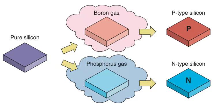
- The first semiconducting material used was the element germanium, however, silicon replaced germanium because it is one of the most common elements on Earth.
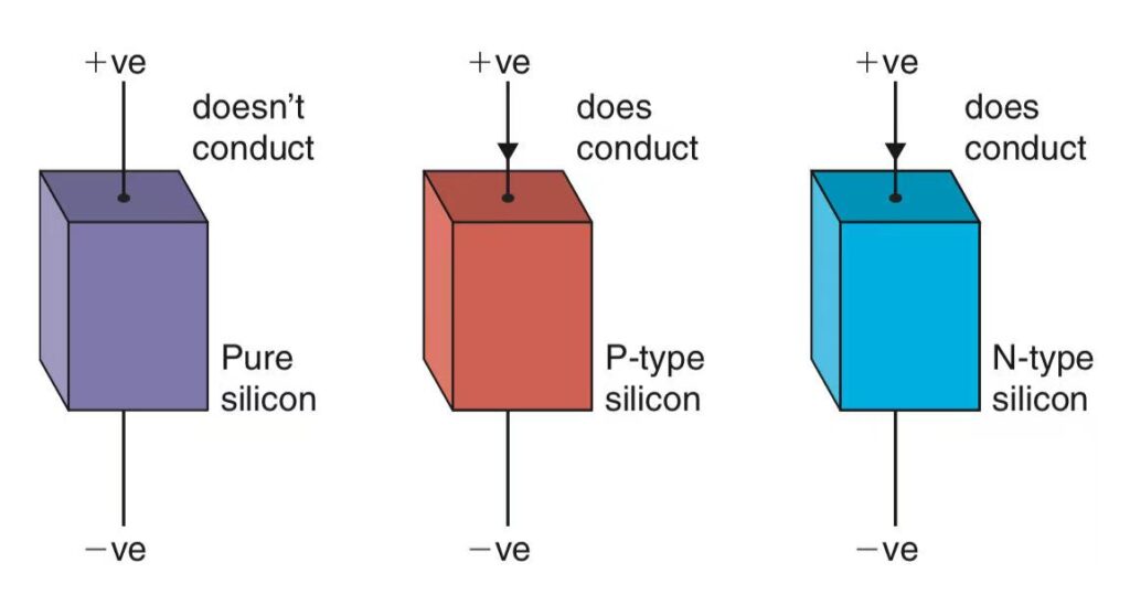
- Pure crystalline silicon acts as an insulator; however, scientists at Bell Laboratories found that by inserting certain impurities into the crystal lattice, they could make silicon act as a conductor. If a piece of pure silicon is surrounded by a gas containing boron or phosphorus and heated in a high-temperature oven, the boron or phosphorus atoms will permeate the crystal lattice and displace some silicon atoms without disturbing other atoms in the vicinity. This process is known as diffusion. Boron-doped silicon is called P-type silicon and phosphorus-doped silicon is called N-type silicon.
- p-type Silicon: p-type silicon is doped with elements like boron, which have one less valence electron compared to silicon. This creates “holes,” or places where an electron is missing, which can move and act like positive charge carriers.
- n-type Silicon: n-type silicon is doped with elements like phosphorus, which have one more valence electron than silicon. This provides extra electrons, which can move freely and act as negative charge carriers.
Semiconductor Diodes
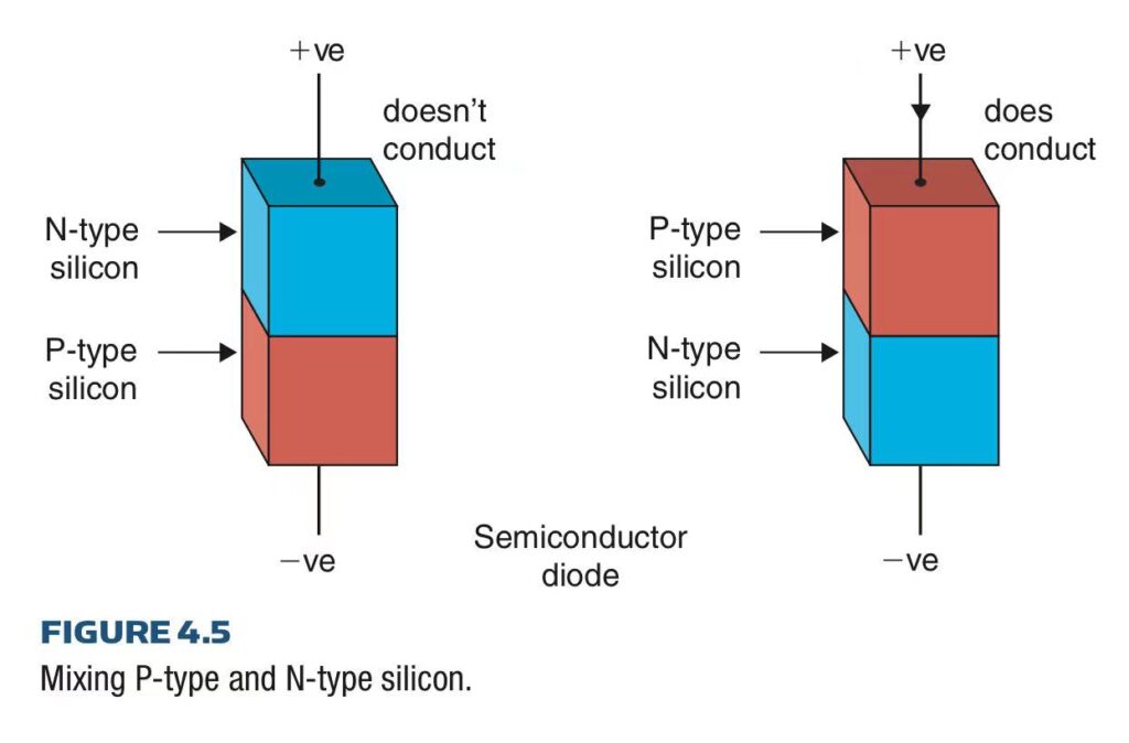
- The silicon with both P-typed and N-type material conducts electricity in only one direction, they are diodes which are unidirectional.
- In one direction, electrons move from the negative terminal to the positive terminal, or from the n-type region diffuse into the p-type region, and holes from the p-type region diffuse into the n-type region. This happens because of the concentration gradient: there are more electrons in the n-type region and more holes in the p-type region.
- The current won’t move in the other direction
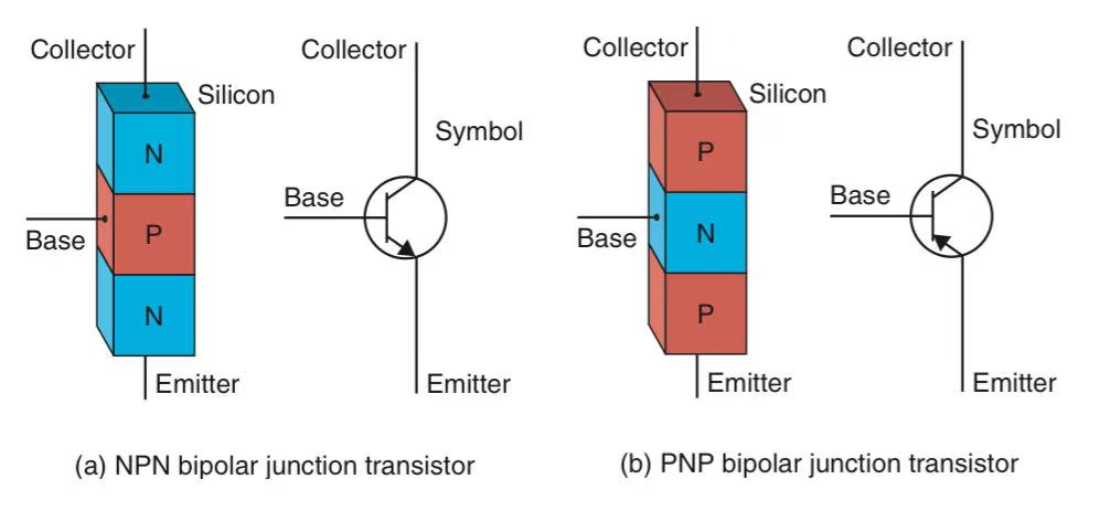
Bipolar Junction Transistors (BJTs)
- BJTs are formed from three pieces of doped silicon called the collector, base and emitter.
- There are two basic types of bipolar transistors called NPN and PNP.
- A transistor can be used as a voltage amplifier, a current amplifier or a switch.
NPN: When the P-type silicon is in the middle, a positive potential difference has to be applied to the base to let it conduct, otherwise it will not conduct.
PNP: When the N-type silicon is in the middle, a negative potential difference has to be applied to the base to let it conduct, otherwise it will not conduct.
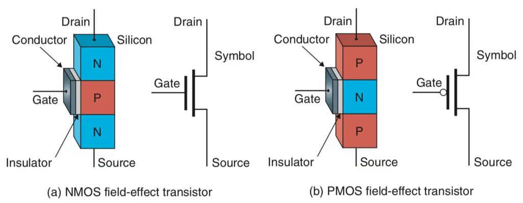
Metal-Oxide-Semiconductor Field-Effect Transistor (MOSFET)
- The MOSFETs, the drain and the source form the data terminals and the gate acts as the control terminal.
- Unlike bipolar devices, the control terminal is connected to a conducting plate, which is insulated from the silicon by a layer of non-conducting oxide.
- When a signal is applied to the gate terminal, the plate, insulated by the oxide, creates an electromagnetic field, which turns the transistor ON or OFF.
- For example, in order to turn the NMOS ON, a positive voltage is applied to the gate. This positive voltage attracts any negative electrons in the P-type material and causes them to accumulate beneath the oxide layer where they form a negative channel.
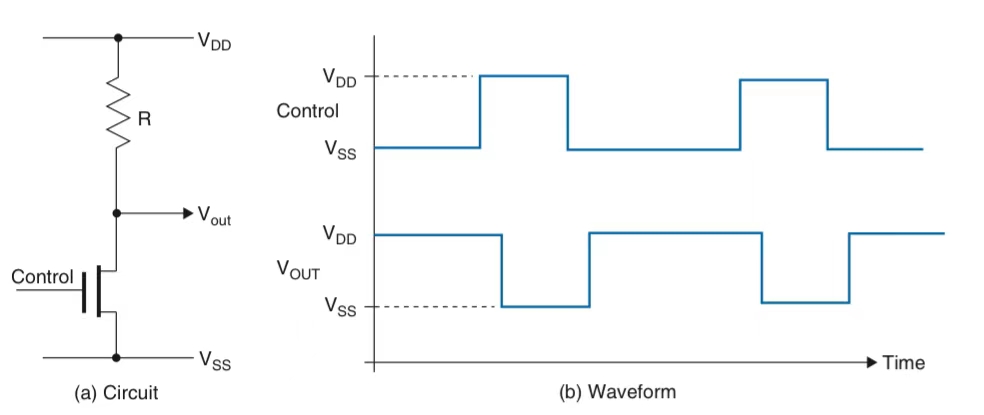
Transistor as a Switch
- When the control input to an NMOS transistor is connected to Vss, the transistor is turned OFF and acts like an OPEN switch
- When the control input is connected to Vdd, the transistor is turned ON and acts like a closed switch.
Gallium Arsenide Semiconductors
- The element gallium has three valence electrons and the element Arsenic has five. A crystalline structure of gallium arsenide can be doped with impurities in a similar manner to silicon.
Benefits:
GaAs is approximately eight times faster than silicon equivalents due to higher electron mobility and it has higher power efficiency.
- GaAs: Gallium arsenide has higher electron mobility than silicon. This means that electrons can move faster through GaAs, leading to higher-speed electronic devices.
- Applications: This property makes GaAs ideal for high-frequency and high-speed applications, such as microwave and millimeter-wave electronics, including radar systems, satellite communications, and high-speed integrated circuits.
Drawbacks:
- Cost: GaAs is generally more expensive to produce than silicon.
- Manufacturing Complexity: The fabrication processes for GaAs are more complex and less mature than those for silicon.
Light-Emitting Diodes (LEDs)
- An LED formed from pure GaAs emits infrared light but it is invisible to the human eye.
- Adding aluminium to form AlGaAs results in red light
- Gallium phosphite gives green light
- Aluminium indium gallium phosphite generates yellow and orange light.
- Gallium nitride gives blue light
Benefits:
- Have a very long life
- generate very pure colors
- extremely energy efficient
Organic LEDs (OLEDs):
They are similar but are based on thin layers of organic molecules, the OLED technology produces self-luminous displays that do not require backlighting. These properties result in compact displays that require very little power and are much thinner and brighter.
BeBOP Chapter 4 Key Note: Semiconductors