RAMs VS ROMs
Read-Only Memory: other components in the system can read data from ROM devices but can’t write new data into them. The ROM contains a sequence of instructions that are used by the CPU to initialize both itself and other parts of the system. This is known as boot-strapping.
Random-Access Memory: Data can be read out of RWM (Read-Write Memory) devices and new data can be written back into them.
ROMs are classed as being nonvolatile because their data remains when power is removed from the system.
RAMs are said to be volatile because any data they contain is lost when power is removed from the system.
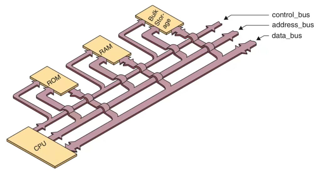
Address Bus & Data Bus
The CPU uses a set of signals called the address bus to point to the memory location it needs. The address bus is unidirectional.
The data is transferred on a set of signals called the data bus which is bidirectional because it can convert information in two directions: from the CPU to the memory and vice versa.
Cells, Words & Arrays
The smallest unit of memory is called a cell, it stores a single bit of data. A number of cells physically grouped together are classed as a word. All the cells in a word are written to or read from at the same time. The core of a memory device is made up of a number of words arranged as an array.
- The width of a memory is the number of bits used to form a word.
- The depth of memory is the number of words used to form the array.
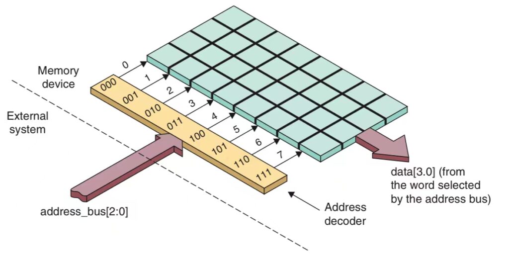
Addressing a Word in Memory
For external components to reference a particular word in the memory, they must specify that word’s address by placing appropriate values onto the address bus and this address is decoded inside the device.
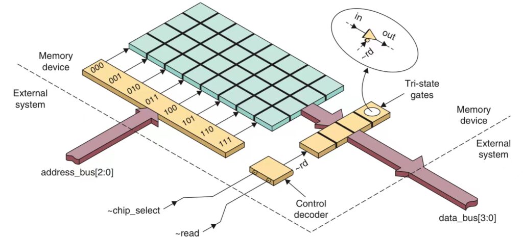
ROM Control Decoding
Due to the fact that multiple memory devices are usually connected to a single data bus, the data from the internal array is typically buffered using tri-state gates. Enabling the tri-state gate allows the device to drive data onto the data bus while disabling them allows other devices to drive the data bus.
The ROM requires two control gates, ~chip_select and ~read which are normally active low. ~chip_select signal indicates to the ROM that its attention is required while the ~read signal is used to control the tri-state gates.
When ~read is inactive, the tri-state gates are disabled and are placed into high-impedance states.
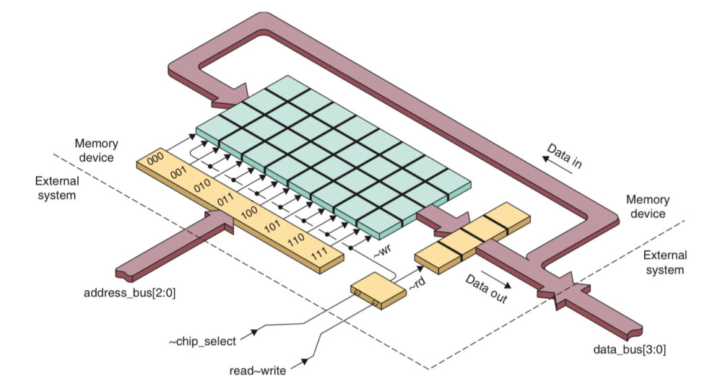
RAM Control with Single Bidirectional Bus
RAMs use a common bus for both writing and reading. the ~read and ~write signals are combined into a read~write signal where logic 1 is associated with a read operation and logic 0 is associated with a write.
Increasing Width & Depth
Individual memory devices can be connected together to increase the width and depth of the total memory.
E.g. two 1024-word devices each 8 bits wide can be connected so as to appear to be a single 1024-word device with a width of 16 bits (increase width) or a 2048-word device with a width of 8 bits (increase depth).
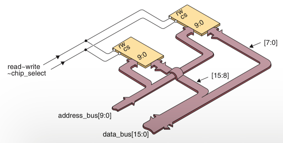
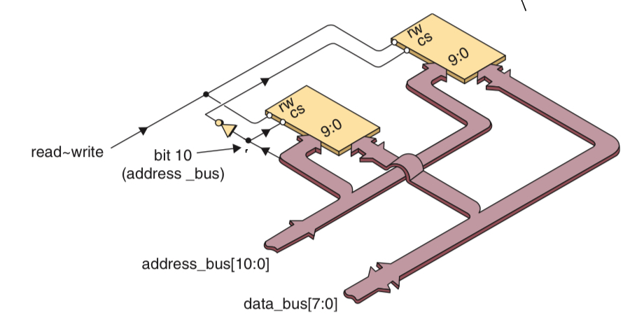
When we increase the depth, the data bus, the read~write control and all the bits in the address bus starting with the second one are common to both memory. However, the Most Significant Bit (MSB) of the address bus is decoded to generate two ~chip_select signals.
Mask-Programmed ROMs
ROM devices are said to be mask-programmed because the data they contain is hard-coded into them during their construction.
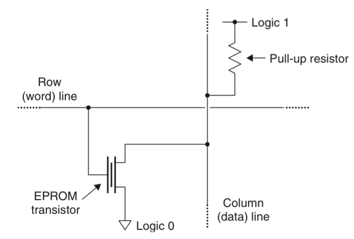
Each column has a single pull-up resistor attempting to hold that column to a weak logic 1 value. Every row-column intersection has an associated transistor and a mask-programmed connection.
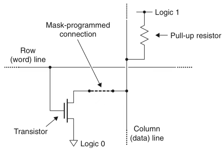
When a row line is placed in its active state, in the case of a cell that includes a mask-programmed connection, activating that cell’s transistor will connect the column line through the transistor to logic 0. By comparison, in the case of a cell that doesn’t have a mask-programmed connection, that transistor will have no effect.
PROMS (Programmable Read-Only Memory)
The Programmable Read-Only Memory devices were created using nichrome-based fusible-link technology.
After manufacture, it is in its unprogrammed state, all of the fusible links in the devices are present. Design engineers can selectively blow undesired fuses by applying pulses of relatively high voltage and current to the device’s inputs. Normally, when placing a row line in its active state will turn on all of the transistors and cause all of the column lines to be pulled down to logic 0, but wherever a fuse is blown, that cell will appear to contain a logic 1.
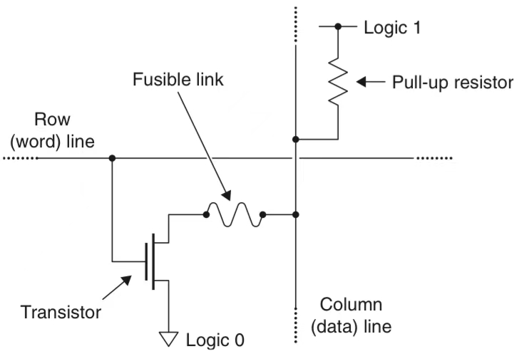
PROMs are said to be One-Time Programmable (OTP), because once you’ve programmed one and blown its fuses, there is no going back. However, they are significantly cheaper for small to medium sized production runs.
EPROMs (Erasable Programmable Read-Only Memory)
Erasable Programmable Read-Only Memory is a device that can be programmed, erased and reprogrammed with new data. An EPROM transistor has the same basic structure as a standard MOSFET transistor but with the addition of a second polysilicon floating gate isolated by layers of oxide.
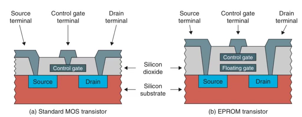
In order to program the. transistor, a relatively high voltage is applied between the control gate and drain terminals. This causes the transistor to be turned hard on and energetic electrons force their way through the oxide into the floating gate in a process known as hot electron injection.
When the signal is removed, a negative charge remains on the floating gate and inhibits the normal operation of the control gate which distinguishes themselves from those cells that have not been programmed. This charge is very stable and will not dissipate for more than a decade under normal operating conditions.
An EPROM cell is erased by dischargin the electrons on that celll’s floating gate. The energy required to discharge the electrons is provided by a source of Ultraviolet radiation. However, the main problems with EPROM devices is the time it takes to erase them, which takes over 20 to 30 minutes.
EEPROMs (Electrically-Erasable Read-Only Memory)
EEPROM devices are electrically programmable by the designer and are non-volatile, but can be electrically erased and reprogrammed. They are approximately 2.5 times larger than an equivalent EPROM cell as it comprises two transistors and the space between them. Similar to EPROM, it contains a floating gate, but the insulating oxide layers in EEPROM are much thinner.
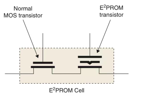
EEPROM can be erased and reprogrammed while remaining resident on the circuit board, so it is referred to as In-System Programmable (ISP)
Flash
Flash is a combination of the best features from EPROM and EEPROM, all variants of it are electrically erasable like EEPROMs. Some. flash devices are based on a single transistor cell and other devices are based on a dual transistor cell.
SRAMs & DRAMs
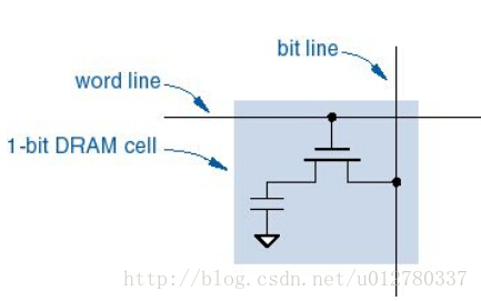
In a dynamic RAM (DRAM), each cell is formed from a transistor capacitor pair. The term dynamic is used because a capacitor loses its charge over time and each cell must be periodically recharged to retain its data. Some DRAM may contain its own internal self-refresh circuitry.
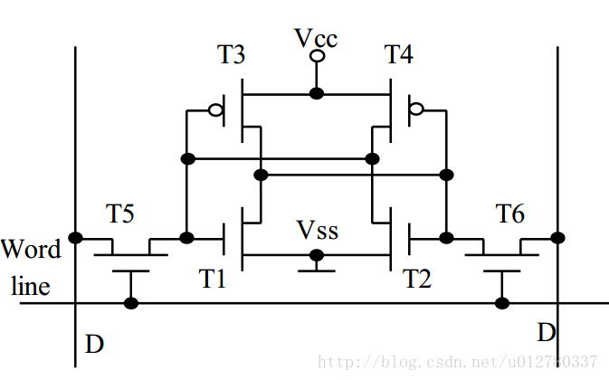
In a static RAM (SRAM), each cell is formed from four or six transistors configured as a latch or a flip-flop. Data will remain unchanged until it is explicitly altered or until the power is off.
SRAMs are much faster than DRAMs but SRAM cell requires significantly more silicon an consumes much more power. DRAM is usually used to satisfy the bulk of a system’s RAM requirements while SRAM is used where fast speed is required like the cache.
SDRAMs
Synchronous DRAM (SDRAM) refers to a memory subsystem that is synchronized to the system clock. It is based on DRAM arranged in multiple banks that are interleaved together and accessed via a multiplexer.
Instead of storing blocks of data in contiguous locations in the same bank of DRAM, in a SDRAM the first word of data would be stored in bank 0, the second word in bank 1, the third word in band 2, and so on. In this way, the interleaved banks of DRAM can be used to store and retrieve data much faster.
ECC Memory
There is always the chance that an error will occur when reading or writing to the memory. Error-Correcting Code memory (ECC) includes the extra bits and special circuitry that tests the accuracy of data and corrects any errors.
MRAMs
Magnetoresistive Random Access Memory (MRAM) are able to store more data, read and write data faster and use less power than any of the current memory technologies. It combines the advantages of each of the other memory devices.