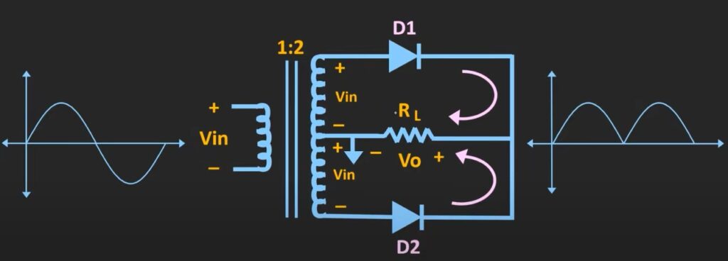
The full wave rectifier allows the use of both half of the input signal as it completely pass the positive half cycle and inverts the negative half cycle.
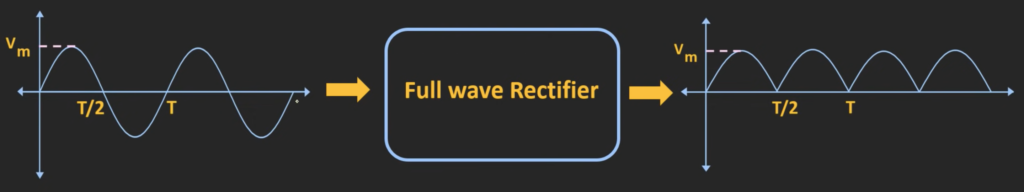
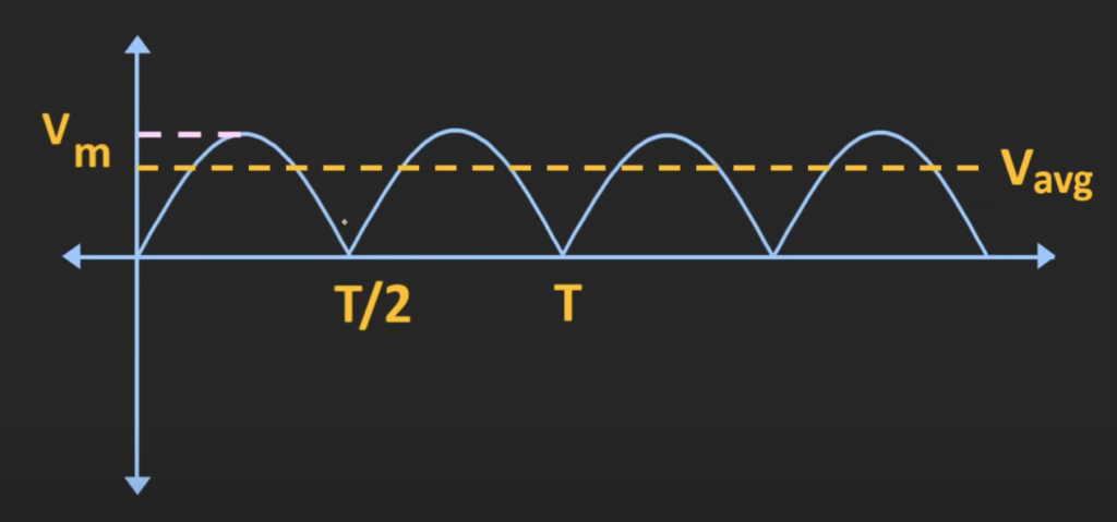
Notice that in the output wave form, the frequency of the output waveform has been doubled, as the wave is repeating itself every T/2 period.
There are two ways to build a full wave rectifier, the center-tapped transformer method and the diode bridge method.
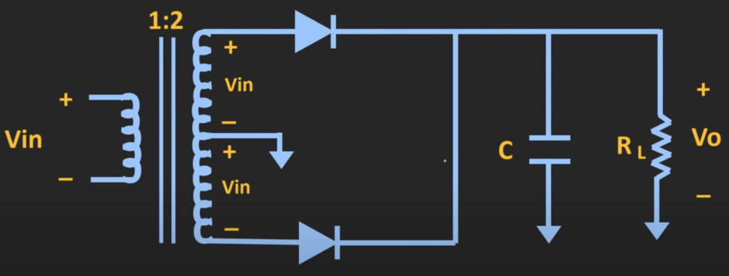
Center-Tapped Transformer
The center-tapped transformer is used at the input side, the center of the secondary winding is grouded. The transformer ratio used in the circuit is 1:2 meaning that if the voltage applied to the primary winding is V, the voltage at the secondary winding would be two times that value.
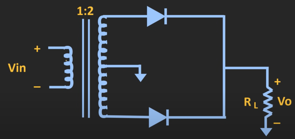
Since the center of the transformer is grounded, the output voltage between the center and one end of the winding will be the same as the input voltage.
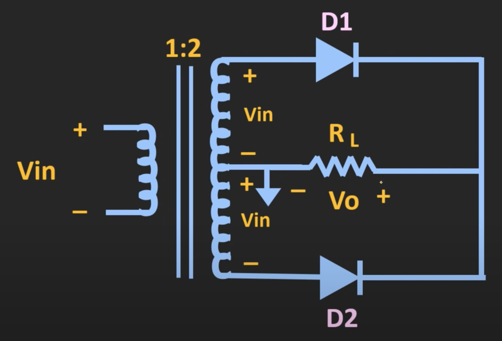
When we apply the sine wave input signal to the circuit, during the positive half cycle, the diode D1 will conduct and D2 will remain reversed biased, so the current would flow from positive to negative through the load. On the other hand, during the negative half cycle, the diode D1 will remain off and D2 will conduct and the current will flow through the load in the same direction.
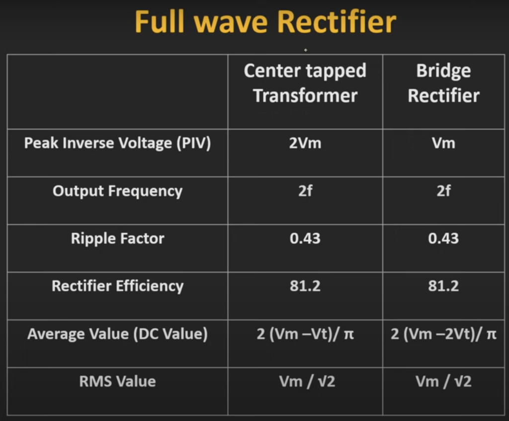
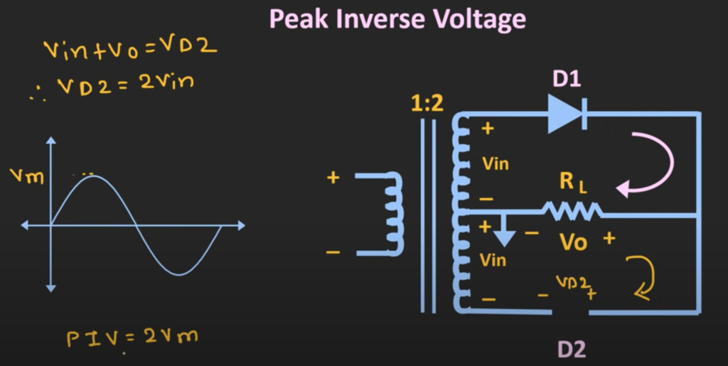
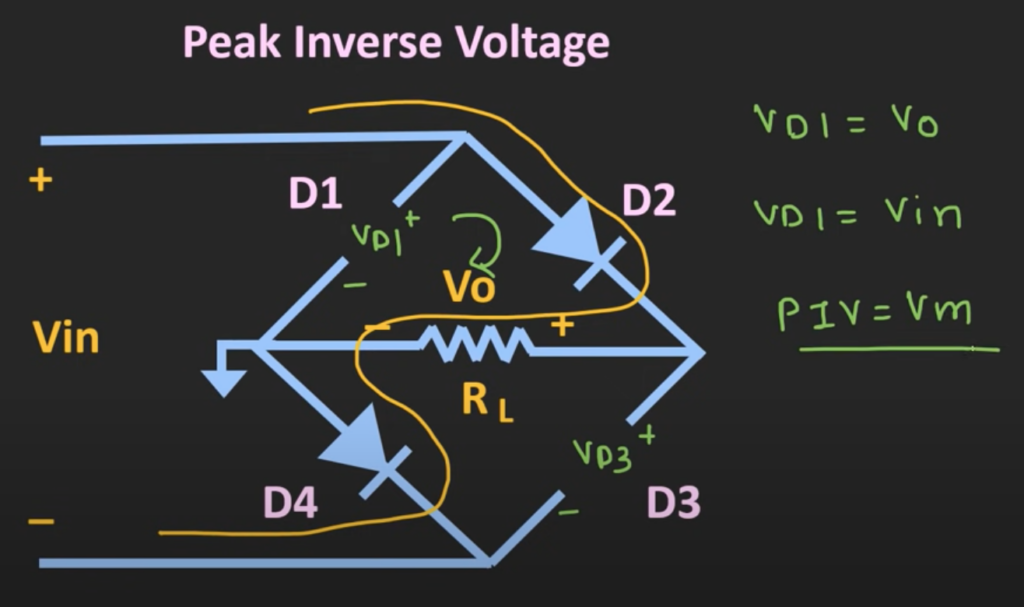
Peak Inverse Voltage
It is the maximum voltage appears in the reversed biased condition. In the positive half cycle, the diode D2 is in the reversed biased condition, by appling the Kirchhoff’s voltage law, we can find out that the input voltage plus the voltage across the load is equal to the voltage across the diode D2. If both diodes are ideal, the voltage across the load resistor will be equal to the input voltage, so the peak inverse voltage of the diode in this circuit is twice the input voltage – 2Vin.
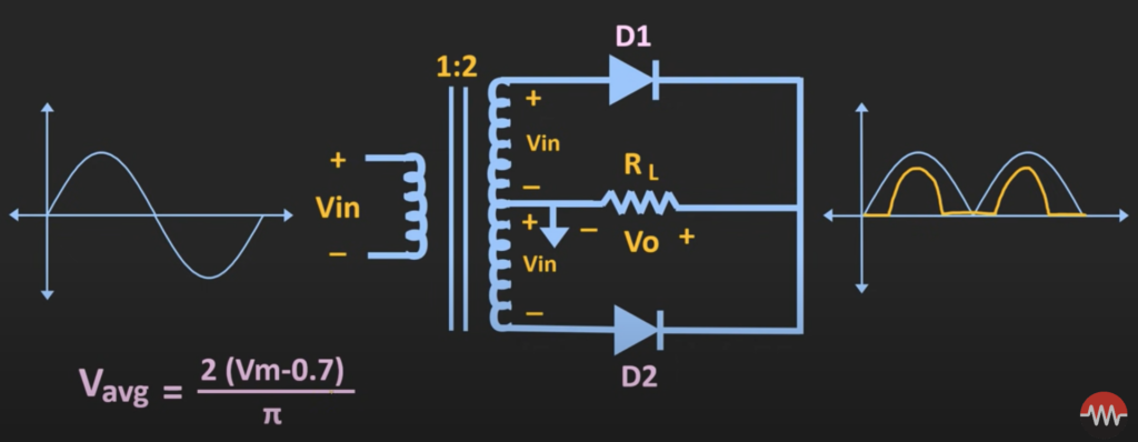
Average Voltage Value
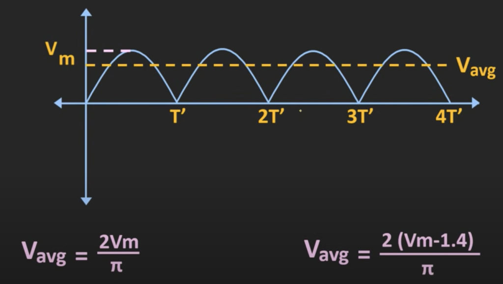
Here, as we are getting an output for both half cycles, the average value for this full wave rectifier will be more than the average for half wave rectifier. To be precise, the average value would be 2V/π which is double the average value of the half wave rectifier.
However, in reality there is also voltage drop in the diodes, the actual curve would look like the yellow one because the diode will conduct only when the applied voltage crosses the threshold voltage. Due to this, the peak voltage will also reduce.
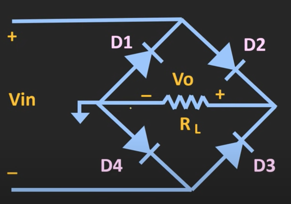
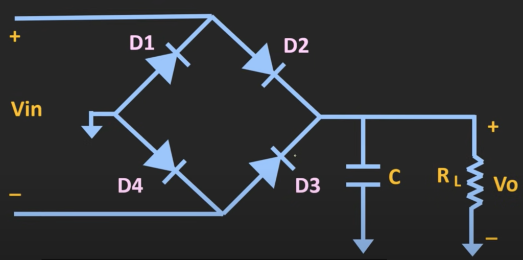
Full Wave Bridge Rectifier
The full wave bridge rectifier consist of four diodes, and due to the fact that it doesn’t contain any transformers, the size of this circuit will reduce.
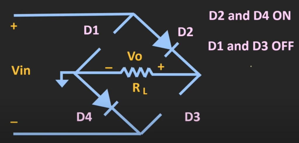
If the sine wave signal is applied, during the positive half cycle, diodes D2 and D4 will conduct while diodes D1 and D3 will remain off. If the D2 and D4 diodes are ideal, the input voltage will appear across the load resistor.
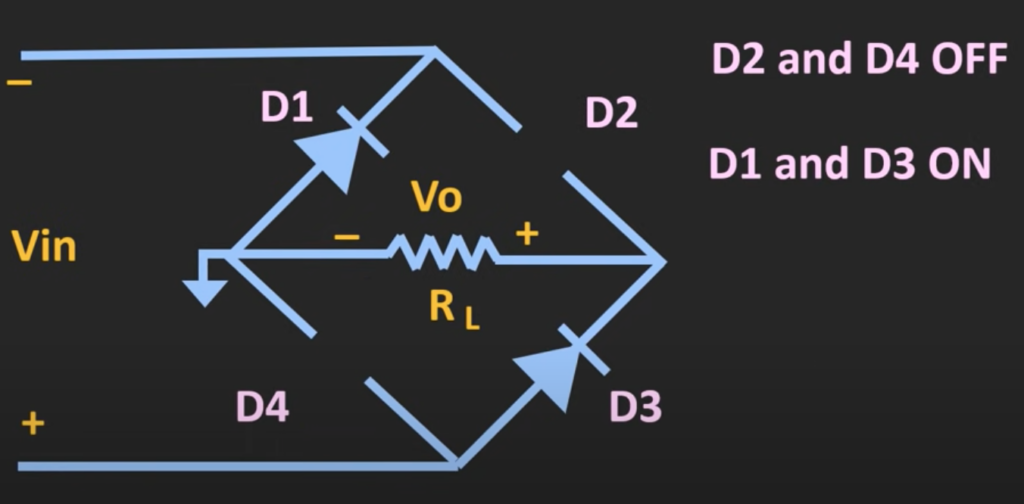
Similarly, during the negative half cycle, the diodes D2 and D4 are off while D1 and D3 are on. As you can see, the direction of flow of current is the same as the direction during the positive half cycle.
Average Voltage Value
If the four diodes in the circuit are all ideal, the average value for the full wave bridge rectifier would be identical to the center-tapped rectifier. However, in reality, there is a voltage drop on both diodes in the circuit, so the voltage drop is larger.
Peak Inverse Voltage
During the positive half cycle, the current flow through diodes D2 and D4, and in diodes D1 and D3 there is an reverse voltage. By appling the Kirchhoff’s voltage law, we can find that voltage at diode D1 will be equal to the input voltage, so the PIV (peak inverse voltage) for the diode D1 would be the input voltage and the same is applied to all other diodes in the circuit.
Filter Circuit
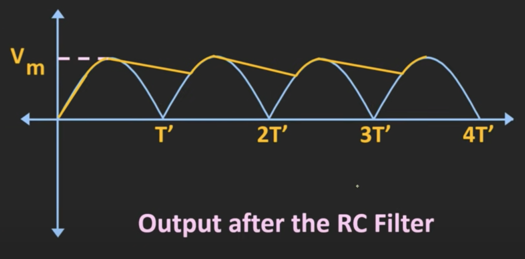
If you look at the output wave form, it is still not completely a DC voltage, because there is still some periodic variation and this variation is known as the ripple. This ripple can be reduced by using the filter circuit at the output of the rectifier. To add the filter circuit is just to connect a capacitor in parallel to the load resistor.
For the center tapped rectifier circuit, during the increasing part of the positive half cycle, this capacitor will charge up to peak voltage, once this capacitor gets fully charged, then the diode D1 will get reversed biased. After the peak voltage, the capacitor discharges through the load resistor. Whenever the voltage of the capacitor just go below the input voltage, it will start to recharge again.
With this filter, the output wave form will look like the yellow curve. Due to the charging and discharging of capacitor we will get this kind of wave form. For better reduction of the ripple, the RC time constant should be much larger than the time period. If the RC time constant is less than the period, the capacitor will discharge very quickly and thus causing more ripple.
Peak to Peak Ripple Voltage
Since it is still not a perfect DC voltage, there is some ripple in the output waveform. This ripple voltage is known as the peak to peak ripple. This voltage can be given by the following expression:
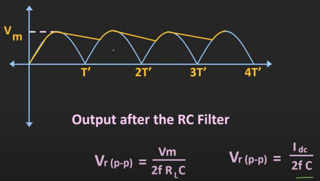
- f is the frequency of the input signal
- R is the resistance of load
- C is representing the capacitor
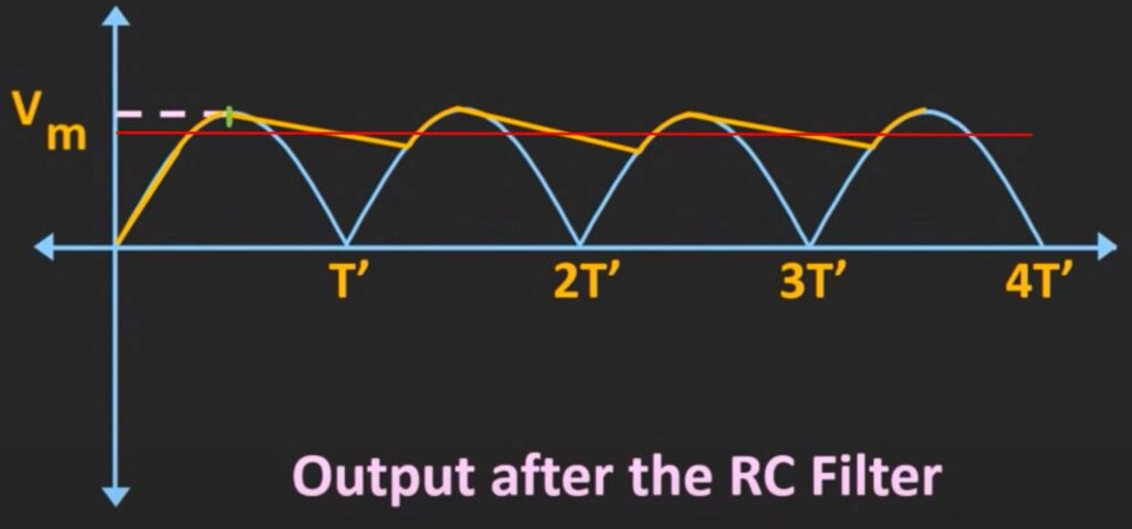
Average Voltage Value
The value of the average voltage of this wave form can be given by the expression V = Vm – V(p-p)/2. It means that the average voltage would approximately be the peak voltage minus half of the peak to peak voltage.
Ripple Factor
The ripple factor is a parameter that defines how well the ripple is removed from the circuit. The ripple factor is the ratio of the RMS (root mean square) value of this ripple divided by the DC voltage. The value for the full wave rectifier is about 0.43 which is a lot lower than the ripple factor for the half wave rectifier which is about 1.21.
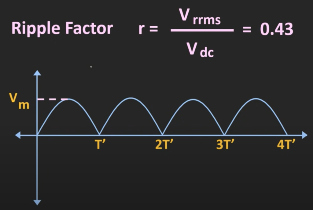
This value can be further improved by using the filter circuit and it can be derived from the following equation:

Efficiency
The efficiency of a rectifier is defined as how well the input AC power is converted to the DC power. For the full wave rectifier, the efficiency is about 81.2% which is drastically improved comparing to the efficiency of half wave rectifier of 40.6%. It double the efficiency.

Summary