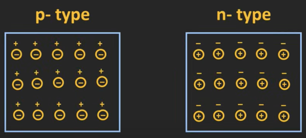
P-type & N-type Semiconductor
P-type & N-type semiconductor by itself acts like a resistor.
Doping one side of the silicon crystal with p-type impurity and the other side of the silicon crystal with n-type impurity creates the PN junction. The PN junction is also called a diode.
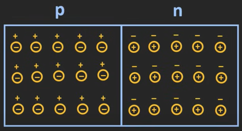
Due to the doping of different impurities, there are a lot of electrons on the N side but very few electrons on the P side. The electrons from the N side would diffuse towards the P side and combine with the holes.
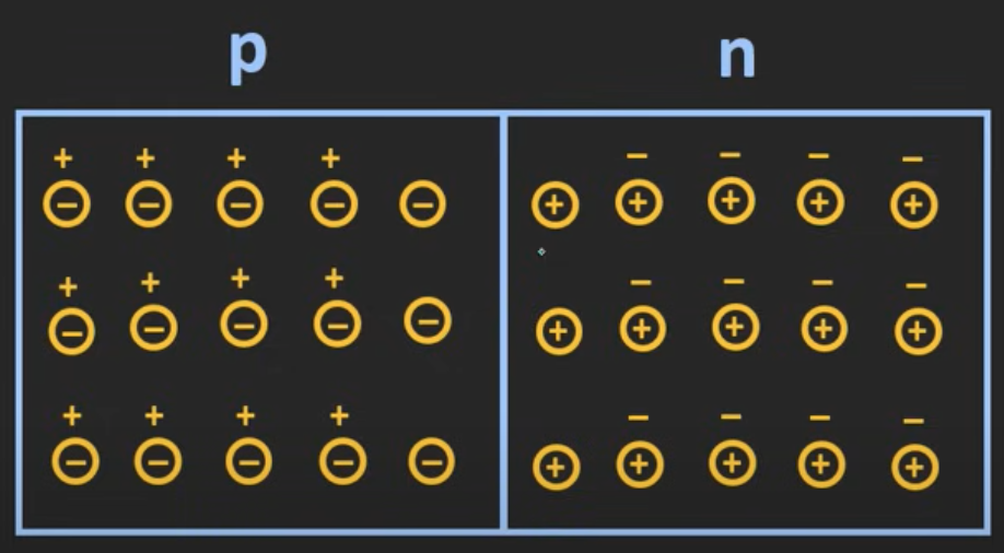
Due to one short of electron in the N side, the pentavalent atom will become a positive ion. Due to capturing an extra electron in the P side, the trivalent atom will become a negative ion. These ions are immobile ions meaning that they can not move.
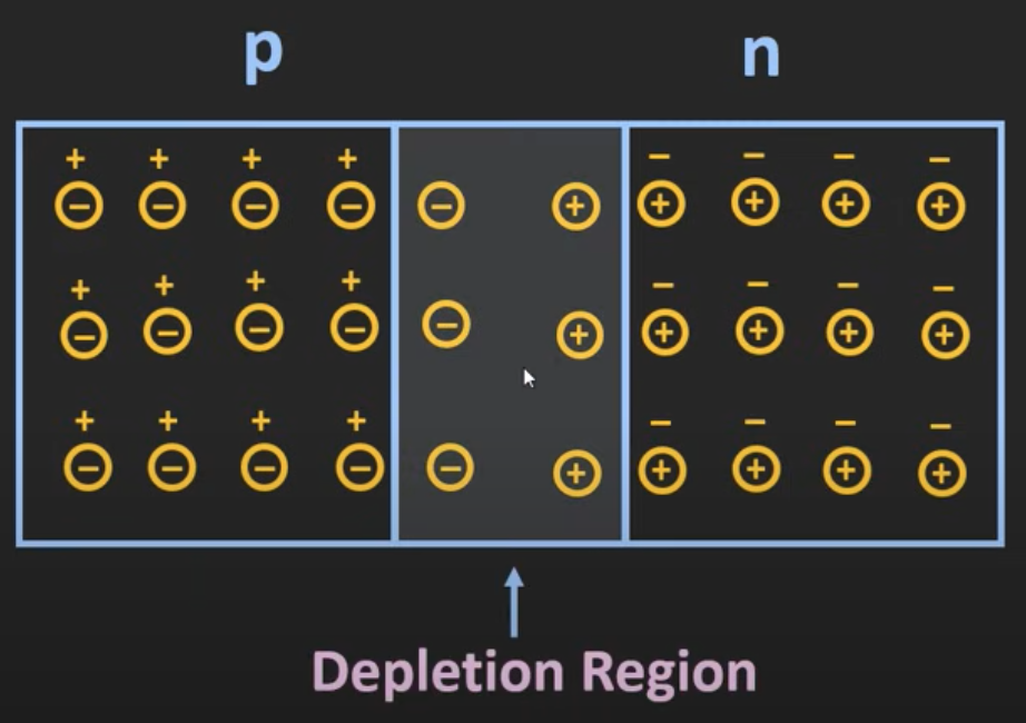
There would be hardly any free-charge carriers near the junction. Due to the combination of P-type and N-type semiconductors, this junction is depleted from free charge carriers, so this region is also known as the depletion region.
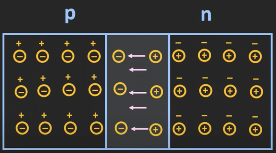
In the depletion region, the ions set up an electric field pointing from the positively charged ions to the negatively charged ions. So, due to this electric field, hardly any electrons from the N side can cross to the P side. These immobile ions create the barrier potential for these majority carriers. This barrier potential is also known as the built-in potential, for the silicon, this potential is about 0.7 V. This voltage is the minimum voltage required for carriers to cross the depletion region.
Unbiased PN Junction
If the external field is applied in the same direction as the built-in electric field, the depletion region will provide more resistance to the majority carrier.
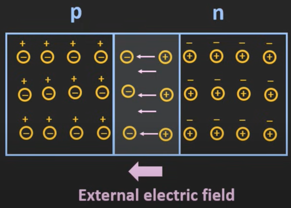
If the applied external field is in the opposite direction as the built-in electric field, the resistance offered by the depletion region will be reduced.
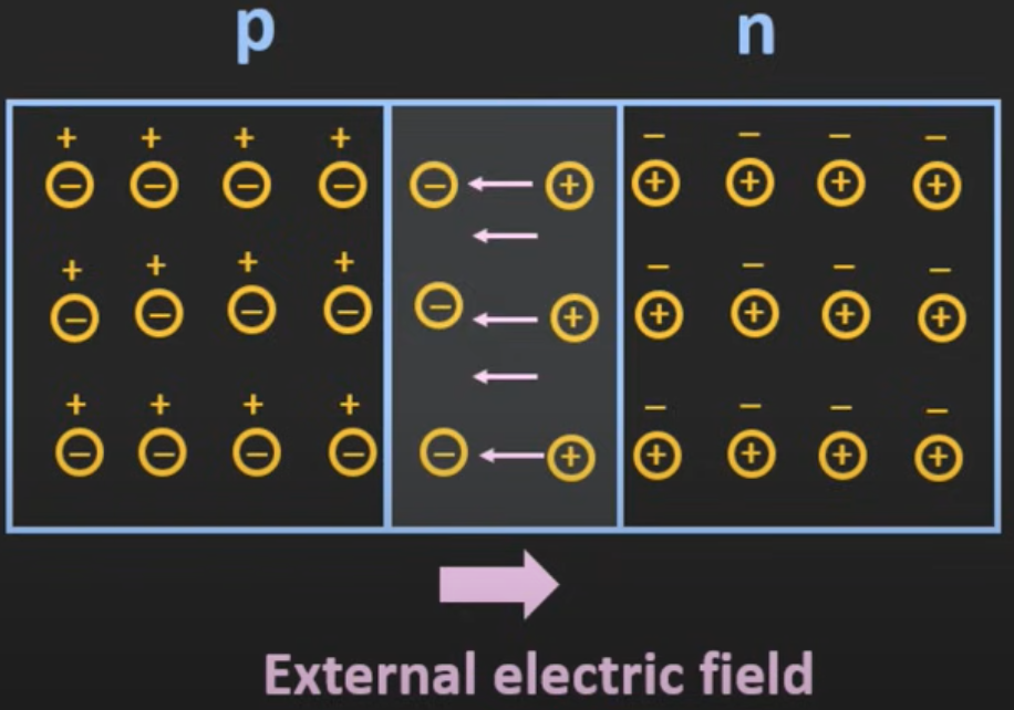
Forward Biased PN Junction
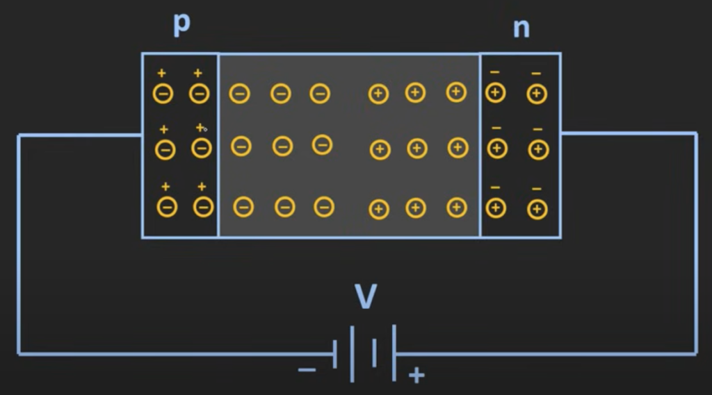
The positive terminal is connected to the P side while the negative terminal is connected to the N side. The external electric field is in the opposite direction of the built-in electric field. The effective electric field will be reduced, and the electrons in the N side and the holes in the P side will be pushed towards the junction. The width of the depletion region will reduce, so the effective resistance will also reduce.
When the applied voltage is more than the barrier potential of the PN junction, the resistance offered by the depletion region will be negligible. So the electrons in the N side can cross the barrier and get attracted to the positive terminal.
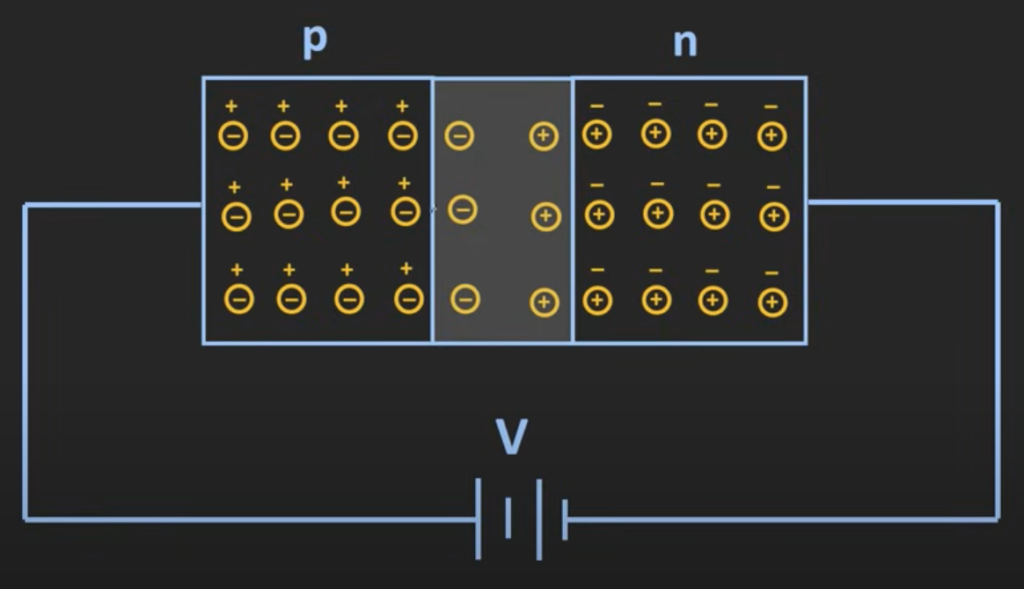
Reverse Biased PN Junction
The negative terminal of the battery is connected to the P side while the positive terminal of the battery is connected to the N side. The electrons on the N side region will get attracted to the positive terminal and the holes in the P side region will get attracted to the negative terminal. So more ions will get created near the junction, and the width of the depletion region will increase thus offering more resistance to these majority carriers.
In the reversed biased condition, we will get a flow of current due to these minority carriers. However, there are very less minority carriers compared to majority carriers, so the magnitude of the current in the reverse baised condition will be very low compared to the forward biased condition.
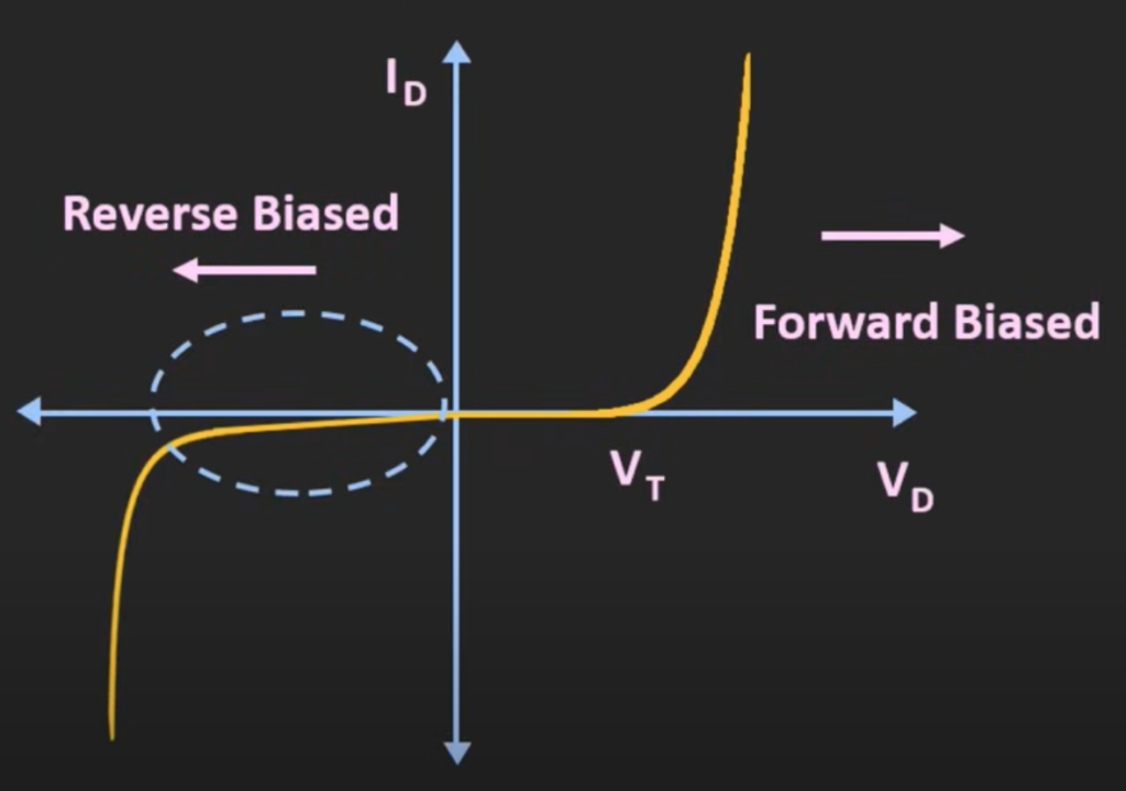
The flow of current in the reverse biased condition is called the reverse saturation current.
Reverse Saturation Current
The reverse saturation current is directly proportional to the temperature. As the temperature rises, the minority carriers charges in the silicon crystal will increase, so the reverse saturation current will also increase. Every 10 degrees rise in temperature, the reverse saturation current almost gets doubled.