This is the symbol for the schottky diode, it is quite similar to the symbol of the normal diode.

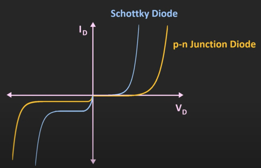
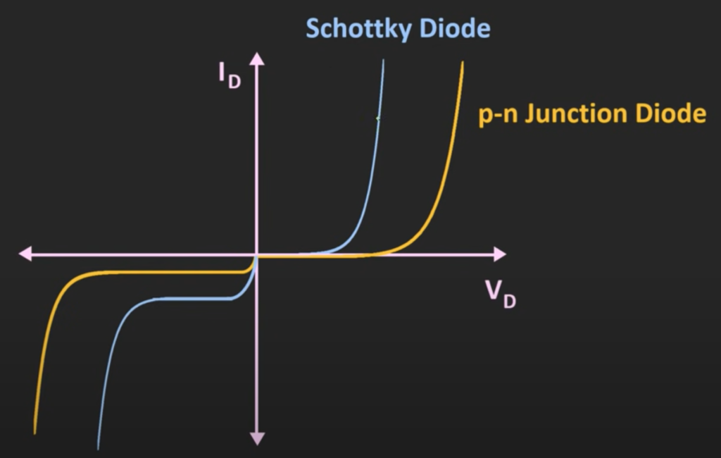
The voltage drop for the schottky diode is about 3 volts to 5 volts which is lower then the voltage drop for the rectifier diode. It can be shown in the V-I graph of the diodes. This low voltage drop has many advantages, particularly in high power applications. This is because the power dissipated in a diode is directly proportional to the voltage drop across it, meaning that by having a lower voltage drop, the power dissipated on the schottky diode is lower and there is also less heat generated.
Fast Reverse Recovering Time / Fast Switching
Reverse recovering time is a term that defines how fast the diode is able to respone to switching, it is related to the switching speed of the diode.
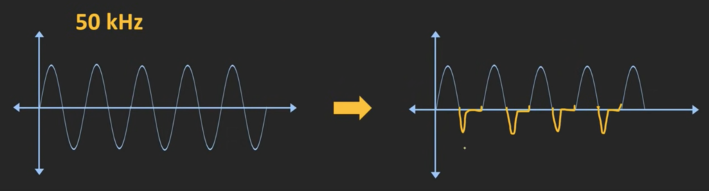
For example, if a AC voltage of frequency 50 kilohertz is inputted into a half wave rectifier built using a normal diode, it won’t be able to surpress the negative half cycle and will get this kind of output wave form. This is because the reverse recovery time for the rectifier diode is large, due to that it will also conduct for some times during the negative half cycle. So, the normal diode doesn’t work at high frequency.
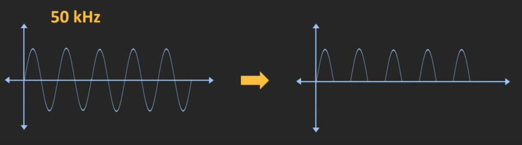
However, if the schottky diode is used, due to its fast recovering time, it will also be able to rectify the high frequency signal. It’s application includes switch mode power supply (SMPS), RF mixer, detector circuits, etc.
High Reverse Saturation Current
One of the limitation of the schottky diode is that it has high reverse saturation current. It is evident from the V-I characteristic of the schottky diode. From the graph, we can see that the breakdown voltage of the schottky diode is less compared to the P-N junction diode, it means that the peak inverse voltage is lower as well. Apart from that, the operating temperature range of the schottky diode is also less.
Construction of the Diode
Unlike the P-N junction in a normal diode, here the metal and semi-conductor junction is formed. In a schottky diode, the semi-conductor used to be a n-type semi-conductor. While for the metal, different host metals like chromium, platinum or tungsten are used. So, in both materials, the electron is the majority carrier.
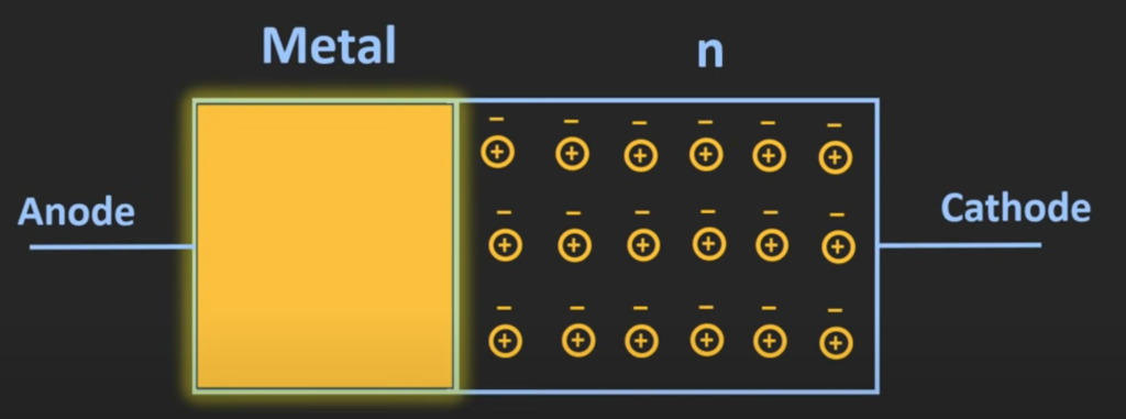
When these two material are joined, the electrons in the n-type material will flow into the metal. The injected electrons have very high energy compared to metal electrons, these carriers are known as the hot carriers. One unique thing about the schottky diode is that the flow of current is only due to the majority carriers, in other words, it is a unipolar device.
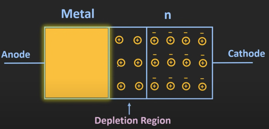
Due to the flow of electrons to the metal, a region near the junction on the n-side will get depleted of the electrons forming a depletion region. The addition of majority carriers in the metal will form a negative wall near the junction. Due to this barrier, the further flow of electrons will be restricted.
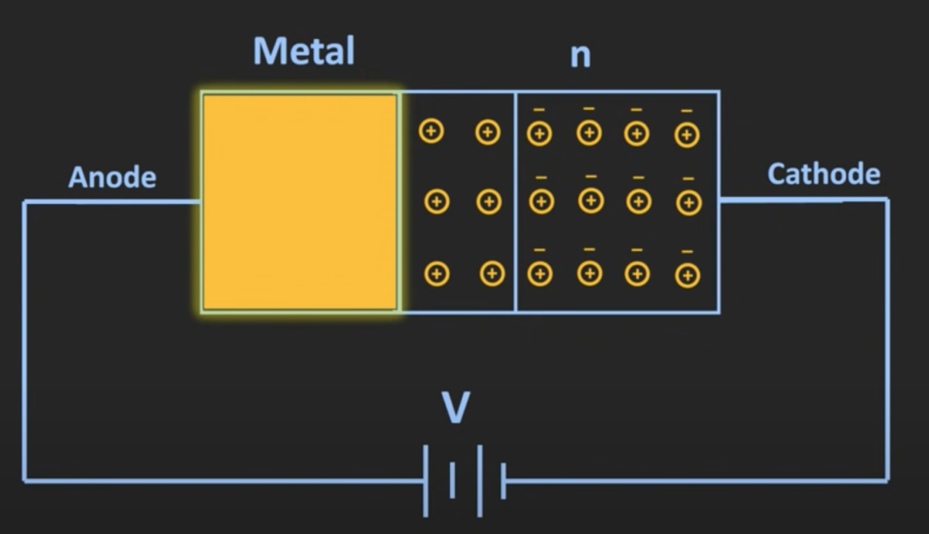
When a forward biased voltage is applied, the strength of this negative barrier will reduce because the electrons will get attracted to the positive terminal. So, the electrons in the n-side will be able to enter the metal, thus there is a flow of electron.
Reverse Recovery Time for P-N Diode
Initially, the P-N diode is in forward biased condition, the electrons which is the majority carrier will enter the p-side region. Once these electrons enters the p-side, they become the minority charge carriers, but due to the applied forward biased voltage, they will continue to move deeper into the p-side region.
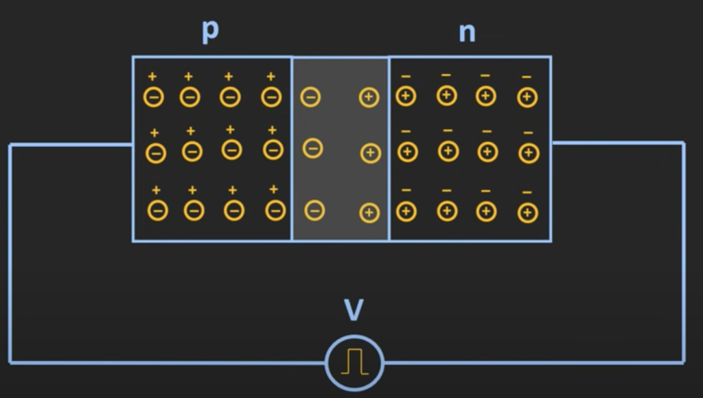
When the applied voltage suddenly changed to the reversed biased condition, idealy, we should not get any current through the P-N junction diode. In the graph below, the current I should become zero after time t1, but there is still some finite current after turning into reversed biased condition. The reason behind it is that whenever we reverse the polarity of the voltage, so the electrons that entered the p-type region will act as a minority carrier and start moving to the positive terminal. Due to this large movement of the minority carriers, there would be a flow of current for a finite amount of time in the reverse direction. This time is known as the storage time, and it defines the time required by the minority charge carriers to return to the majority carrier state.
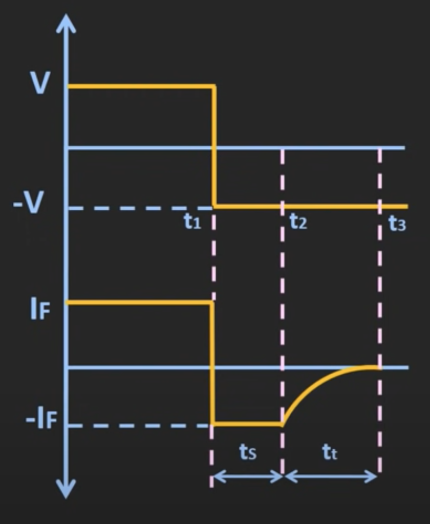
Once the storage time is passed, the reverse current will start reducing and eventually becoming zero. This time between t2 and t3 is known as the transition time. The sum of the storage time and the transition time is known as the reverse recovering time.
In terms of a schottky diode, there is no minority charge carriers, so the storage time for it is negligible. So, thats why it can operate at high frequency.