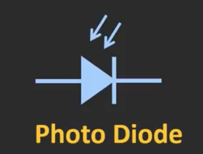
The photo diode is a semiconductor device which converts the incident light into electrical current. Their application includes optical communication system, television, remote control, etc. On this symbol, there is two arrow comming into the diode, it indicates that whenever the light falls on this diode, then it generate the photo current. Unlike the normal rectifing diode,the photo diode is used in the reversed biased mode.
Working Principle
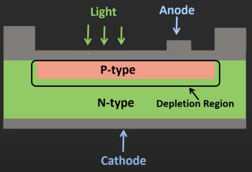
This picture shows the internal structure of the photo diode.
We know that, whenever the diode is working in the reversed biased condition, there will be very little reverse saturation current flowing through the diode. This flow of current is caused by the minority charges.
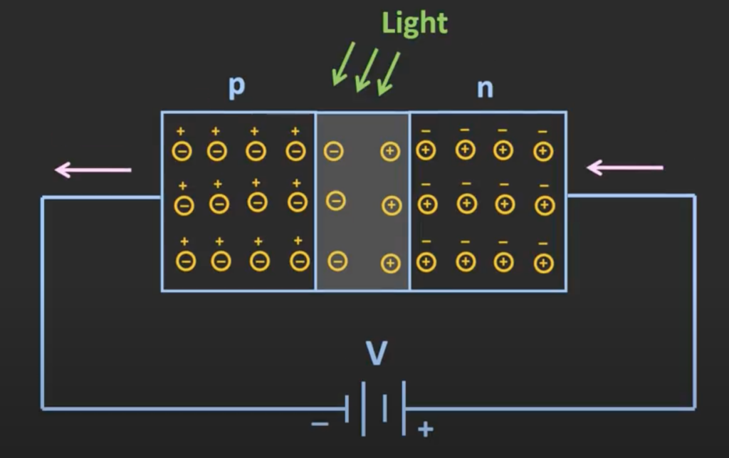
In the case of a photo diode, whenever light of sufficient energy falls onto the photo diode, they can knowck off the atoms’ bound electron in the depletion region.
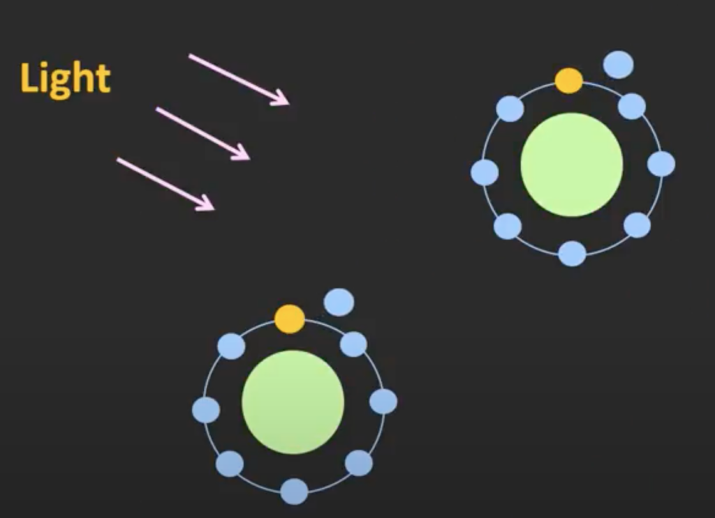
Since more holes are be created, then more electron hole pair will also occur in the depletion region. Some of these electron hole pair will recombine together but others will contribute into the current.
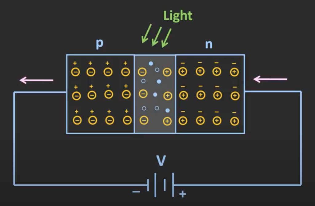
As we know, there is a built in electric field that is already existing in the depletion region of the diode. For the picture above, this electric field is directing from the P side to the N side. It means that the electrons from the P type material want to enter the N type material. These electrons are attracted towards the positive terminal of the cell. On the other hand, the holes in the N side will get attracted to the negative terminal. Due to the incident light, these electrons would be able to cross the depletion region. Once they crosses the depletion region, they will get attracted by the external force of the applied voltage. In this way, they will contribute to a flow of current called photo current. So, whenever light is falls onto the photo diode, in addition to the small reverse saturation current, there will also be photo current.
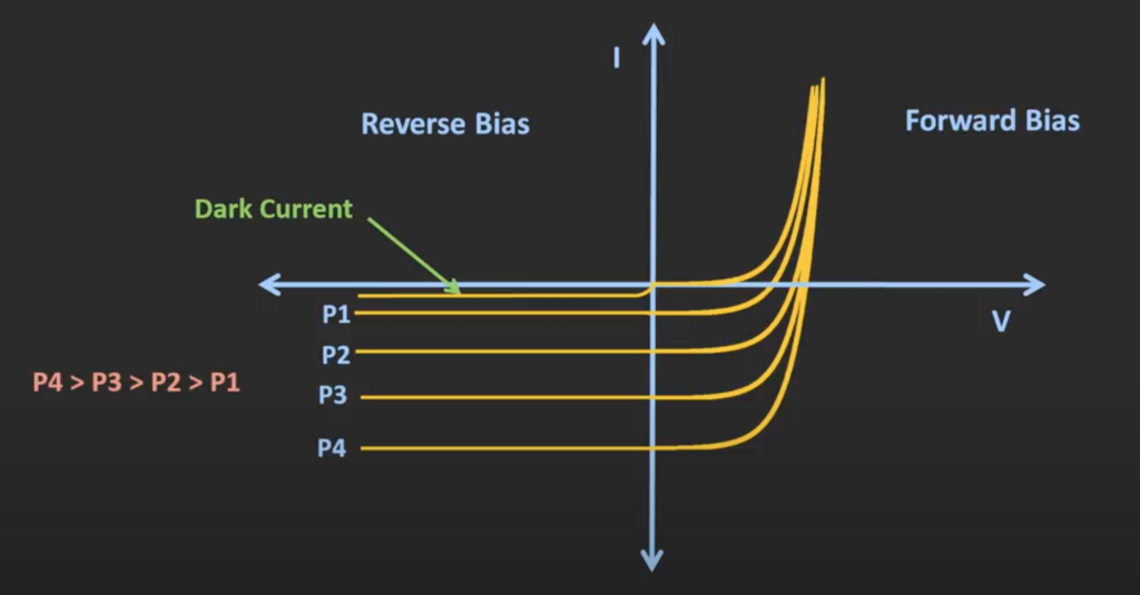
Normally, the reverse saturation current used to be in the range of micro ampere, but for the photo current, it varies with the intensity of light. The picture above shows the V-I characteristic graph of the photo diode, where P1, P2, P3 and P4 represent the intensity of the light. We can clearly see that as the light intensity increases, the photo current will also increase. Moreover, if no light is falling on the diode, there is only reverse saturation current, it is called the dark current in a photo diode. This dark current should be as small as possible because it act as a noice for the photo current.
Photon Energy
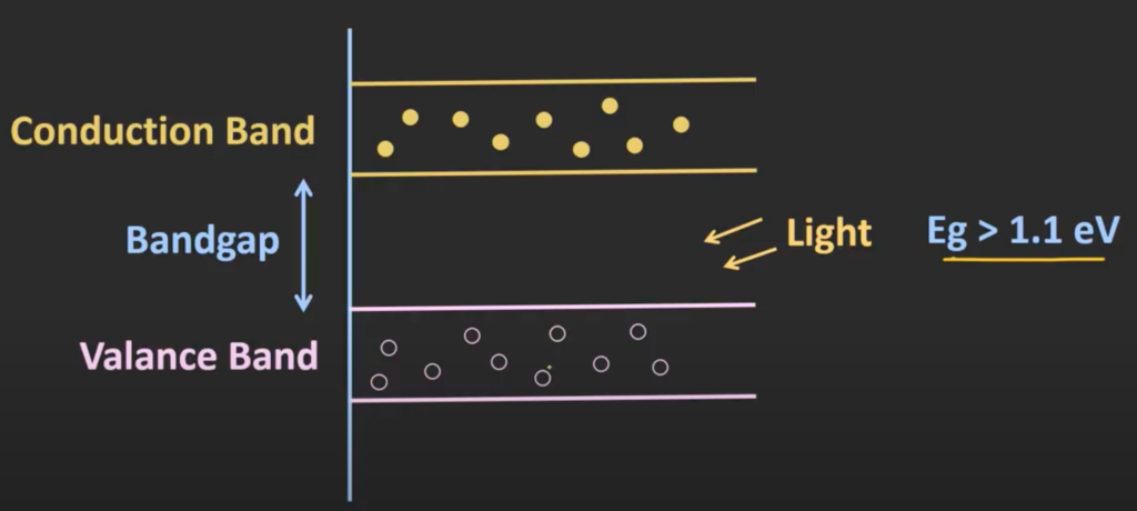
In order for the photo diode to work properly, the photon energy needs to be sufficient enough. For a silicon diode, the energy of the photon should be greater than 1.1 Electric Volts (eV) which is the bandgap energy, so that a electron hold pair gets generated.
As we know, the energy of a photon is expressed using this equation: E = hc/λ
- E: Energy
- h: Planck’s constant
- c: Speed of light in vacuum
- λ: Wavelength of light
It means that the generated photo current is related to the wavelength of the incident light. For a silicon diode, the wavelength should be between 400 nm to 1100 nm to generate a photo current.
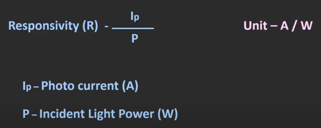
For any photo diode, with a given intensity of light, how much photo current will be generated is represented using the term responsivity (R). It is the ratio of the generated photo current to the power of the incident light. Responsivity is measured in A/W (Ampere/Watts). It is one of the most important parameter for this diode.
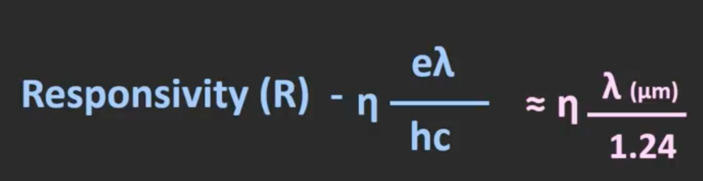
The responsivity can be expressedusing this function, where
- η: Quantum efficiency (Expressed by the equation below)
- λ: Wavelength of incident light
- c: speed of light
- e: charge of electron
- h: Planck’s constant

The following image is the responsivity curve of diodes, it is a fuction of wavelength and also depends the material the photo diode is made of. The responsivity for the silicon diode varies from 400 nm to 1100 nm, in other words, the silicon diode works in the visible spectrum.
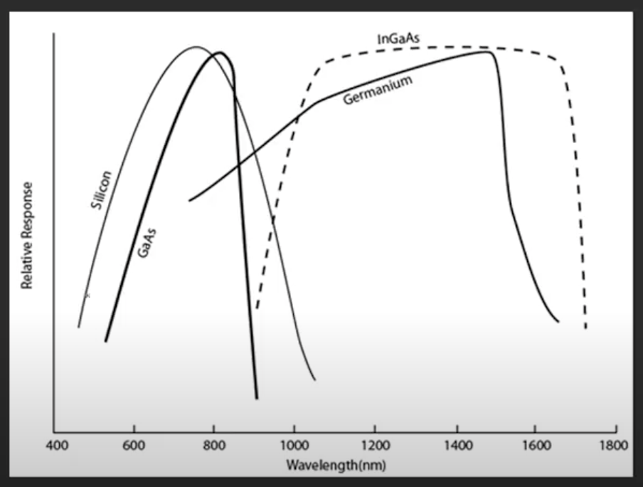
This resistivity curve slightly enhances whenever the photo diode is used in the reversed biased direction. This is because in the reversed biased condition, the depletion region gets wider. Due to that, the chance of absorbing a photon in this region increase.
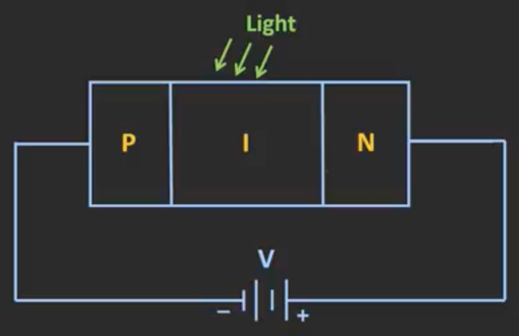
PIN Photo Diode
The PIN photo diode is similar to the PN junction photo diode but it has a larger intrinsic layer between the P and N type. During the reverse biased condition, the entire intrinsic layer will act as a depletion layer. Due to the enhance in depletion region, there is high chance of photon getting absorbed in this region.
Response Time
The response time is how fast the diode can response to the optical pulse. This parameter is really important in fast switching situation, e.g. optical communication. The response time is either represented using the rise time or the fall time. The rise time is the time required for a pulse to rise from 10 percent to 90 percent of its steady value.
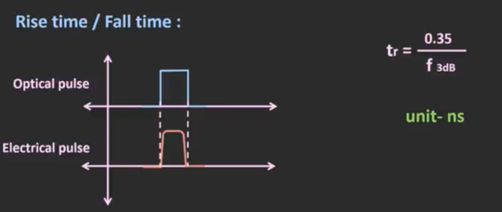
The rise time is usually represented in nano seconds, it is affect mainly by the RC time constant of the circuit. R is the equivalent resistance of the photo diode and the load resistor, C is the equivalent capacitance of the photo diode.
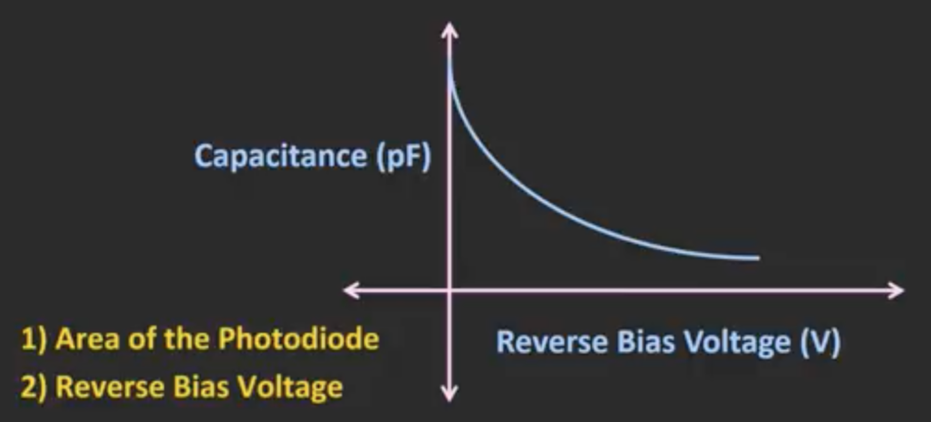
The photo diode capacitance is the junction capacitance of the photo diode. It depends on the area of the photo diode and the applied reversed biased voltage of the photo diode. So as the area of the photo diode increase, the response time will also increase. (C = εA/d) When the applied reverse biased voltage increase, the depletion region will get wider, due to that the distance increase, thus the junction capacitance will reduce.
Photovoltaic Mode
In this mode, no biasing is applied to the photo diode, so the photo current increases linearly with the incident light. The generated photo current is converted into voltage. By connecting the photo diode to the ground ensures that it remains at the zero biasing voltage. In this mode, the dark current is small but the response time for it is slow, therefore not suitable for fast switching applications.
Photoconductive Mode
In the photoconductive mode, the photo diode is reversed biased, the depletion region will increase, so the junction capacitor would reduce. In this case, the dark current would be large but the response time would be small.