NMOS & PMOS & CMOS
- Logic gates can be created using only NMOS or only PMOS transistors
- Complementary Metal Oxide Semiconductor (CMOS) makes use of both NMOS and PMOS transistors connected in a complementary manner.
NOT & BUF Gate Using MOSFETs
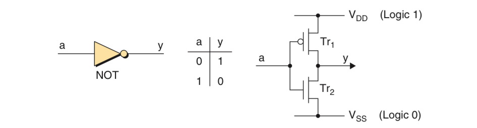
- In Tr1, the small circle on the control input of the transistor indicates a PMOS, which means that this transistor has an active-low control.
- The lack of the circle on the control input of transistor Tr2 indicates an NMOS, which means that this transistor has an active high control.
When we connect the input a to Vss, the transistor Tr1 is turned ON, transistor Tr2 is turned OFF, and output y is connected to Vdd. When we connect the input a to Vdd, the transistor Tr1 is turned OFF, transistor Tr2 is turned ON, and the output y is connected to Vss.
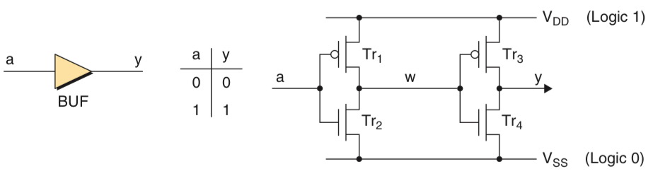
- The BUF gate is constructed from two NOT gates connected in series, which means that it requires four transistors.
- In this case, a logic 0 applied to input a is inverted to a logic 1 on internal signal w, which is subsequently inverted back again to a logic 0 on output y, and vice versa.
- BUF gate may be used for a number of purposes for example to isolate signals, to provide increased drive capability or to add an element of delay.
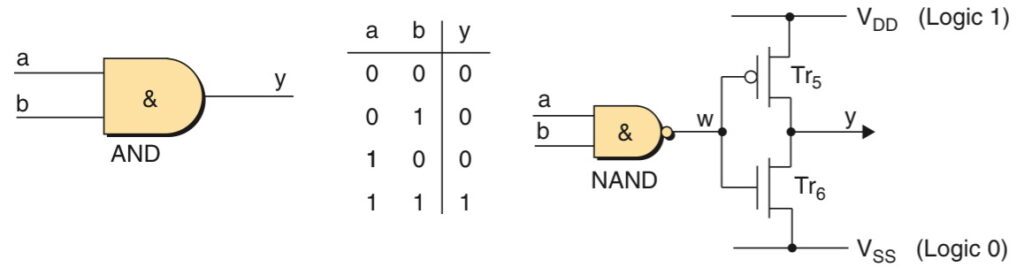
AND & NAND Gates
- It is easier to implement an inverting function than its noninverting equivalent.
- Inverting functions typically require fewer transistors and operate faster than their noninverting counterparts, which can obviously be an important desire consideration.
When both a and b are presented with logic 1s, transistors Tr1 and Tr2 are turned OFF, transistors Tr3 and Tr4 are turned ON, and output y is connected to logic 0 via Tr3 and Tr4. Any other combination of inputs results in one or both of Tr3 and Tr4 being turned OFF and one or both of Tr1 and Tr2 being turned ON, so output y will be connected to logic 1.
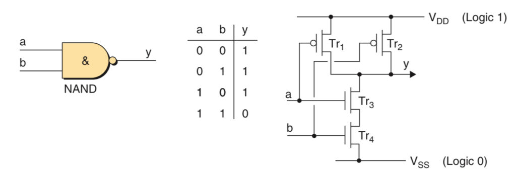
The AND gate is formed by inverting the output of a NAND gate with a NOT, so it requires 6 transistors, 2 more than NAND.
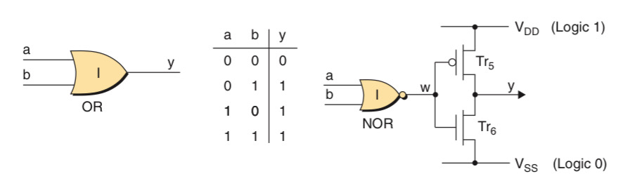
NOR & OR Gates
When both a and b are set to logic 0, transistors Tr3 and Tr4 are turned OFF, transistors Tr1 and Tr2 are turned ON, and output y is connected to logic 1 via Tr1 and Tr2.
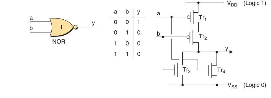
OR gate is formed by inverting the output of NOR gate with a NOT gate.
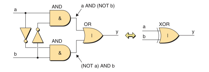
XOR & XNOR Gate
- “Either a or b, but not both”
- The 2-input XOR gates would require 22 transistors if it is made from NOT, AND, and OR gates, which is very inefficient.
For the XNOR gate, when input b is presented with a logic 0, transistor Tr4 is turned OFF, transistor Tr3 is turned ON, and output y is connected to the output of the NOT gate via Tr3. Thus, when input b is logic 0, output y is the inverse of the value on input a. On the other hand, when input b is presented with a logic 1, transistor Tr3 is turned OFF, transistor Tr4 is turned ON, and output y is connected to input a via Tr4. Thus, when input b is logic 1, the output y has the same value as input a. The XOR gate uses the same idea.
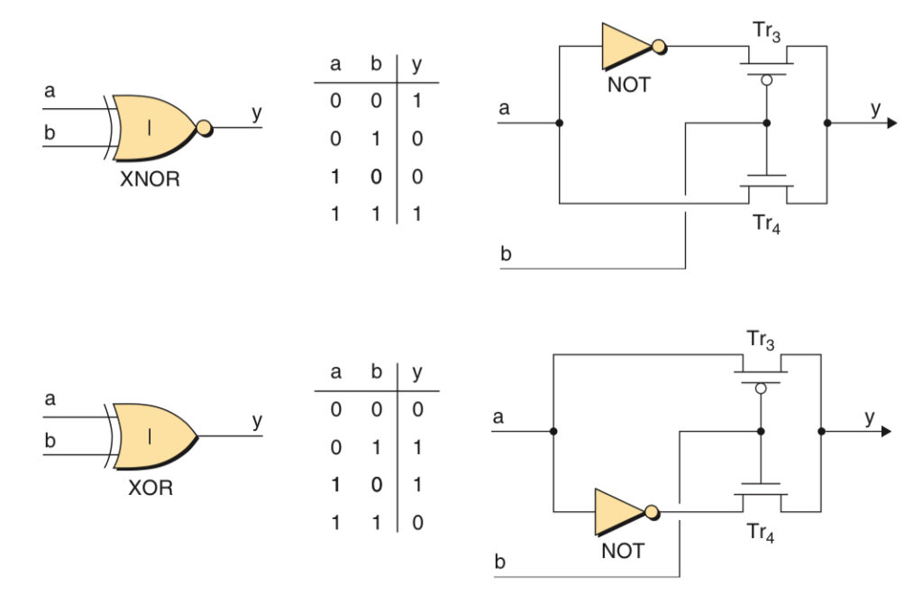
Pass-Transistor Logic
- In BUF, NOT, AND, NAND, OR and NOR gates, the input signals and internal data signals are used only to drive control terminals on the transistors.
- By comparison, in XOR and XNOR, some transistors are connected in such a way that input and internal data signals pass between their data (source and drain) terminals. This technique is known as pass-transistor logic and can minimize the number of transistors required.
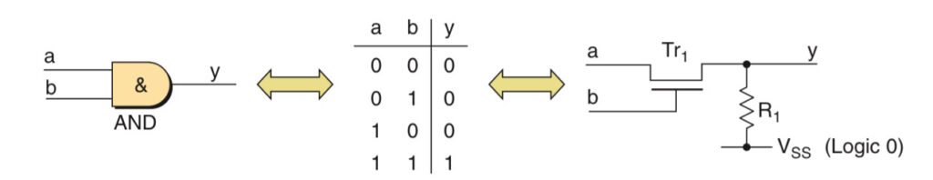
AND using Pass Transistor Logic:
The resistance of R is assumed to be sufficiently high that its effect on output y is that of a very weak logic 0. When input b is presented with a logic 0, the NMOS transistor Tr1 is turned OFF and y is “pulled down” to logic 0 by resistor R. When input b is set to logic 1, Tr1 is turned ON and output y is connected to input a, it leaves y at the same logic as a because the input from a will overdrive the effect of resistor R.
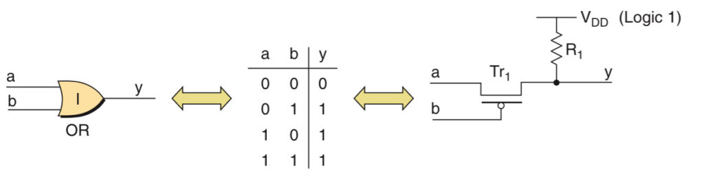
OR using Pass Transistor Logic:
The resistance R is assumed to be sufficiently high that its effect on output y is that of a very weak logic 1. A logic 1 applied to input b turns the PMOS transistor Tr1 OFF and output y is “pulled up” to logic 1 by resistor R. When input b is presented to logic 0, Tr1 is turned ON and output y is connected to input a.