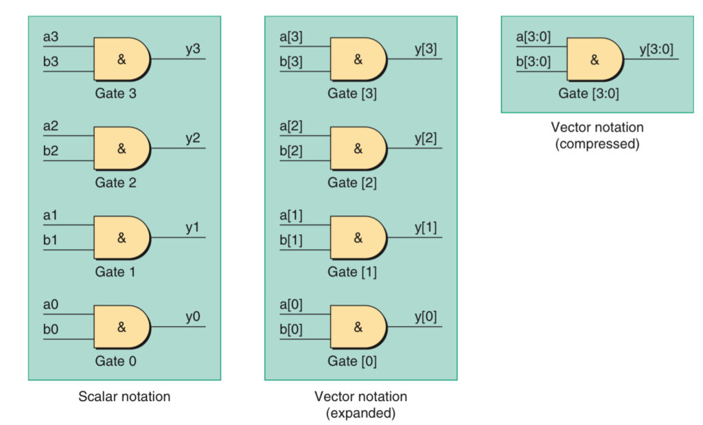
Scalar and Vector Notation
A single signal carrying one bit of binary data is known as a scalar entity. A set of signals carrying similar data can be gathered together into a group known as a vector. A key advantage of vector notation is that it allows all of the signals comprising the vector to be easily referenced in a single statement, it can thus reduce the size and complexity of a circuit while also increasing its clarity.
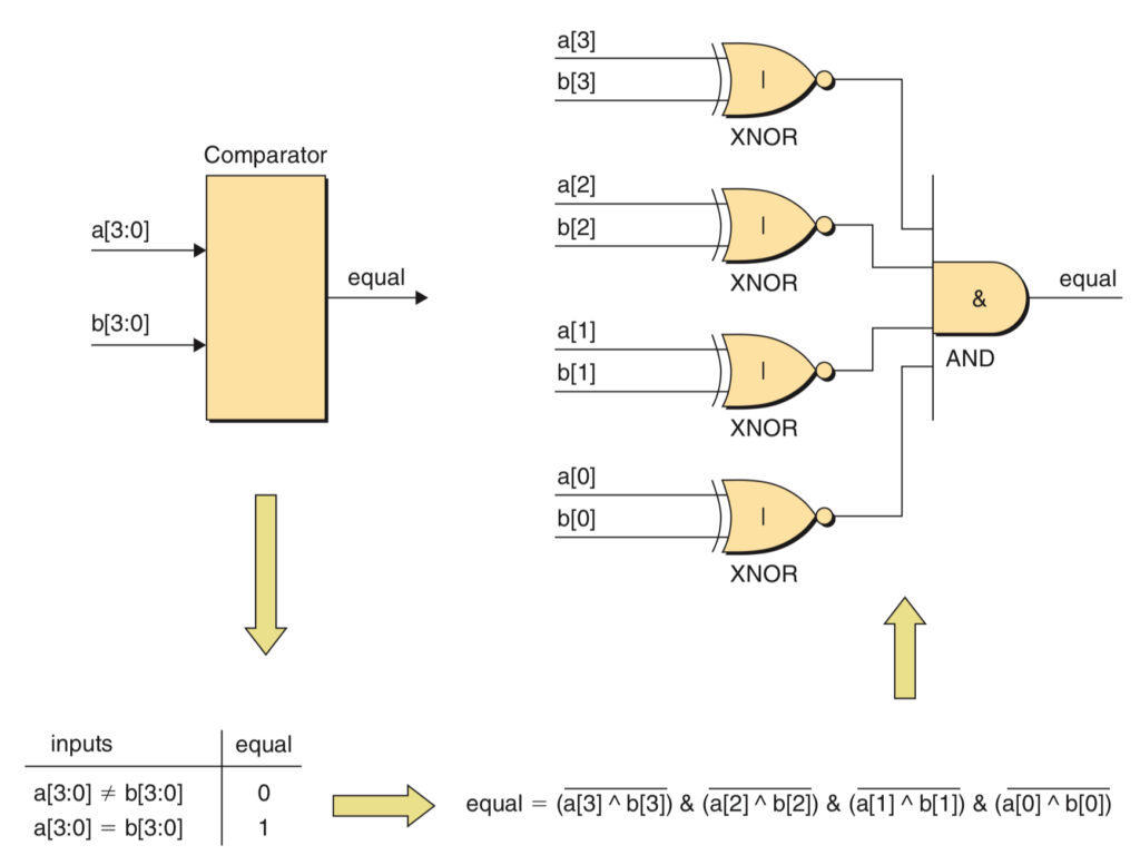
Equality Comparators
Equality comparators are used to compare two sets of binary values to see if they contain the same data. The values on a[3] and b[3] are compared using a two-input XNOR gate, if the values on the inputs to it are the same, then its output will be 1, but if the values of the two inputs are different, the output will be 0. All the outputs of the XNOR gate are connected to the input of an AND gate, if any of the inputs to the AND gate are 0, the two vectors are different and the output of the AND gate will be 0.
Multiplexer
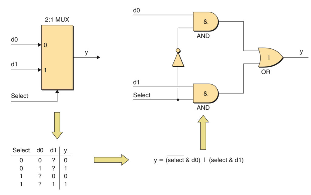
A multiplexer uses a binary value or address to select between a number of inputs and to convey the data from the selected input to the output. For example, a 2:1 multiplexer means that one binary is selected between two. When the select input is logic 0, the output from the function depends only on the value of the d0 data input, and we don’t need to care about the d1 input, and vice versa.
Larger multiplexers can also be made, e.g. 4:1 multiplexers with four data inputs and one output require two select inputs to choose between the four inputs. 8:1 Multiplexers with eight data inputs and one output require three select inputs to choose between the inputs.
Decoders
A decoder uses a binary value or address to select between a number of outputs and to assert the selected output by placing it in its active state.
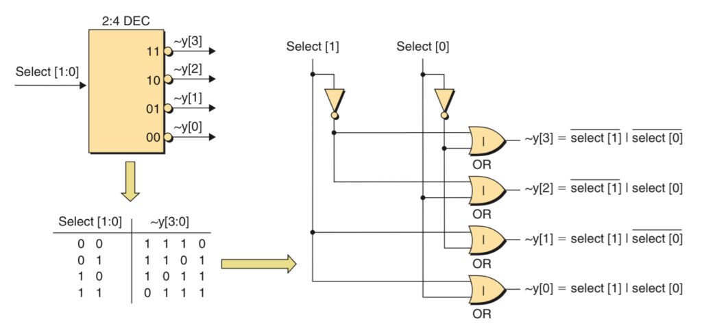
The truth table shows that when a particular output is selected, it is asserted to a 0, and when that output is not selected, it returns to a 1. Since the outputs are asserted to 0s, this device is said to have active low outputs, meaning that its active state is considered to be logic 0. The active low nature of this function is also indicated by the small circle associated with the symbols’ outputs and the tilde character prefixing the output names.
Inputs and Outputs: n inputs and 2 to the power of n outputs, with only one output active at a time.
Tri-state Function
The tri-state functions are a special category of gates whose outputs can adopt three states: 0, 1, and Z. The tri-state buffer’s symbol is based on a standard buffer with an additional control input known as the enable.
The Z character in the truth table represents a state known as high-impedance in which the gate is not driving either of the standard 0 or 1 values. In fact, in the high impedance state, the gate is disconnected from its output.
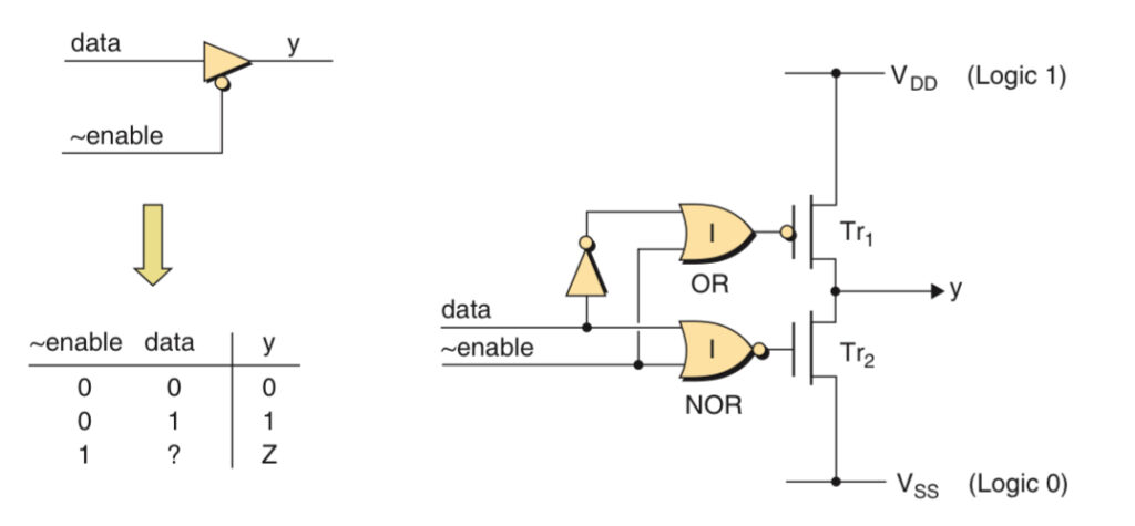
In this case, when the ~enable input is presented with logic 1, the output of the OR gate is forced to logic 1 and the output of the NOR gate is forced to logic 0, thereby turning both the Tr1 and Tr2 transistors OFF, respectively, so the output y is disconnected from both Vdd and Vss and is therefore in the high impedance state.
Applications:
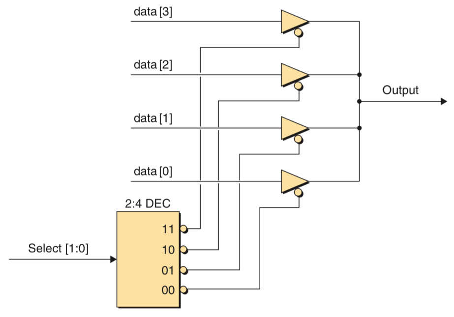
Tri-state buffers can be used in conjunction with additional control logic to allow the outputs of multiple devices to drive a common signal. In the picture below, the 2:4 decoder with active low outputs will only enable one of the tristate buffers at a time, the enabled buffer’s output will become the common output and the remaining tri-state buffers will be forced into their tri-state condition.
Combinational VS Sequential Functions
Combinational Function: The logic values on the function’s outputs are directly related to the current combination values on its inputs.
Sequential Function: The logic values on that function’s outputs depend not only on its current input values but also on previous input values. The output depend on a sequence of input values.
Reset-Set Latch (NOR implementation)
The name of the inputs reset and set indicate the effect they have on the q output, when reset is active q is reset to logic 0, and when set is active q is set to logic 1. The q and ~q outputs are known as the true and complementary outputs, the value on ~q is the inverse or complement of the value on q. The only time ~q is not the inverse of q occurs when both reset and set are active at the same time.
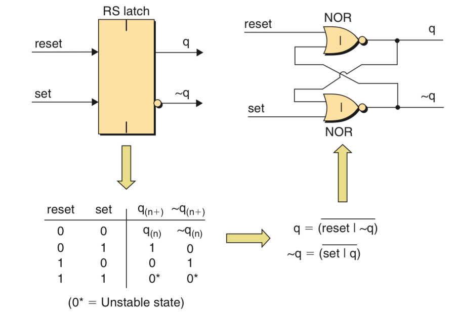
The RS Latch’s ability to remember previous input values is based on a technique known as feedback, meaning that the output of the previous input is being fed back as an additional input into the current function.
Reset:
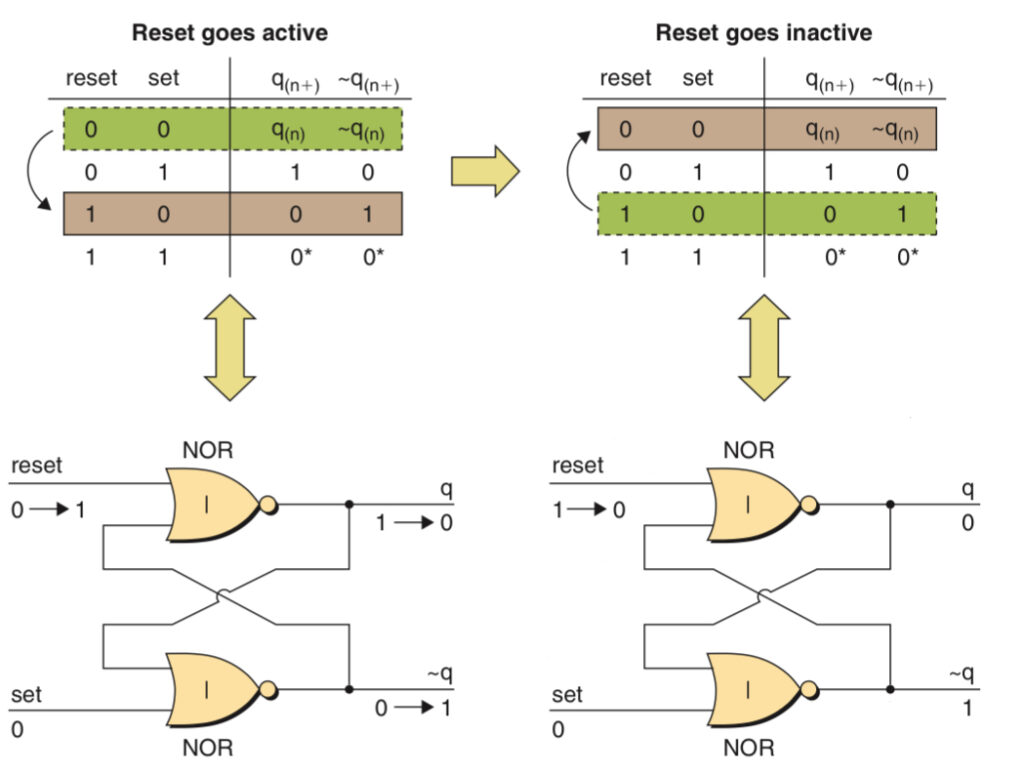
When the reset input turns active or logic 1 is inputted from reset, it turns q to 0. The logic 0 from q together with the logic 0 from the set will turn the ~q to 1. Logic 1 from ~q and logic 1 from the reset through the NOR gate will again make the output q to logic 0 which it already is. Thus, a self-sustaining loop has been established. A similar process also occurs when the reset is turned to an inactive state.
Set:
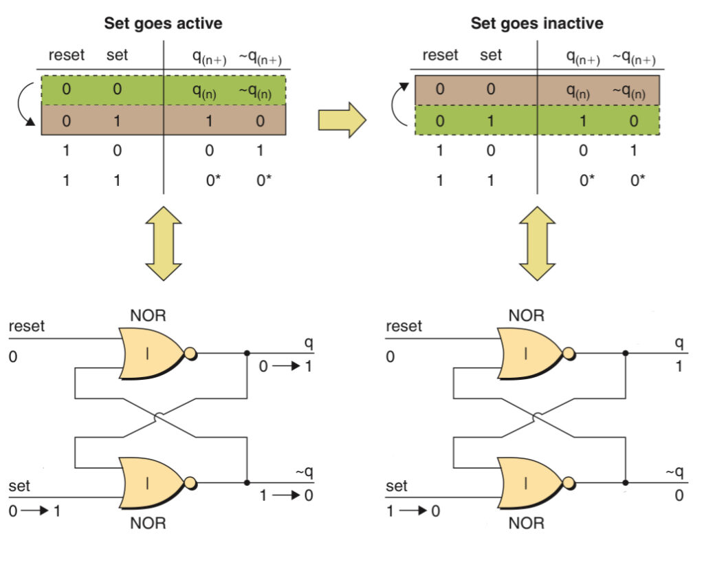
The input from the reset is 0 and the ~q is 0, the output q generated by them through the NOR gate would be logic 1. Logic 1 from q together with logic 1 from from the active set input through the NOR gate will turn the ~q to 0 which is the opposite of q. Both ~q fed back to the first NOR gate and input from reset are 0, thus turning q to 1 which it already is. Thus, a self-sustaining loop has been established. A similar process also occurs when the set is turned into an inactive state.
Unstable Condition:
The unstable condition occurs when both the reset and set inputs are active at the same time. the 1 on reset forces the q output to 0 and the 1 on set forces the ~q output to 0. The 0 on q is fed back to the second gate and the 0 on ~q is fed back to the first gate.
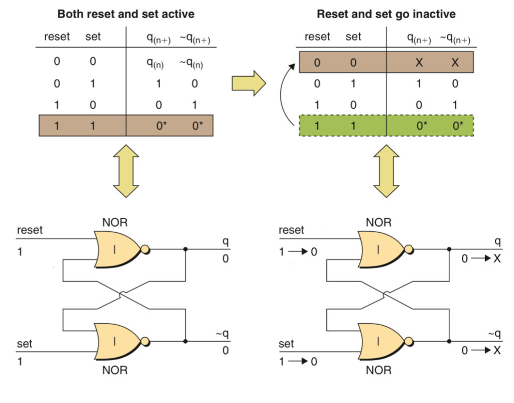
When both reset and set go inactive simultaneously, the logic 0 on reset and set are combined with the 0 values fed back from q and ~q, each gate sees both of its inputs at 0 and therefore both gates output logic 1. When the output of the first gate goes to 1, this value is fed back to the input of the second gate. At the same time, the output of the second gate is fed back to the input of the first gate. Both gates therefore drive their outputs to 0. The circuit now has entered a metastable condition in which the output oscillates between 0 and 1. However, there will always be some differences between gates and their delays, so the function will eventually collapse into either reset or set condition.
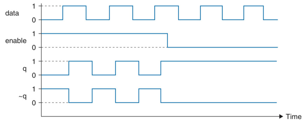
D-Type Latches
Data-type latches can be constructed by attaching two AND gates and a NOT gate to the front of an RS latch. When the enable input is in its active state (logic 1), output q will always be the inputted data and ~q will be the opposite of it. If the data input changes while enable is still active, the outputs will respond to reflect the new value.
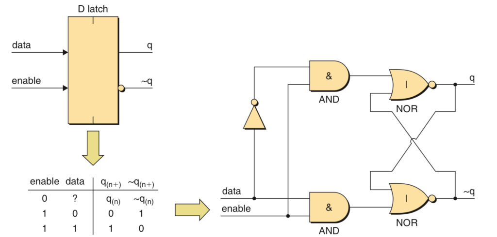
When the enable input returns to its inactive state (logic 0), it forces the outputs of both ANDS to 0, and any further changes to the data input would have no effect, so the back-to-back NOR gates will remember the last value they saw from the data input.
D-Type Flip-Flops
A transition from logic 0 to 1 is known as a rising edge, a transition from logic 1 to 0 is known as a falling edge. In D-type flip flop, data is loaded when an edge occurs on the clock input, so it is edge sensitive. The chevrons symbol (“>”) indicates that it is edge sensitive input.
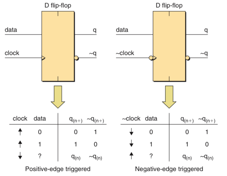
- An inactive edge on the clock leaves the contents of the flip-flops unchanged
- Clock input controls when the value at the data input is sampled and stored. On the rising edge of the clock, the value at the data input is sampled. The output q is updated to this value.
- Some D-type flip-flop also have additional inputs reset and set, Reset forces q to 0 and ~q to 1, while set forces the q to 1 and ~q to 0 irrespective of the value of input.
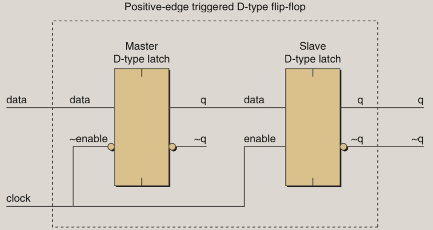
D-type flip-flop can be formed using two D-type latches in series. One of the D-type latch has an active low enable and the second has an active high enable. When one is enabled, the other is disabled, so that the data could be stored in the D-type flip-flop.
Shift Registor
Shift registers facilitate the shifting of binary data one bit at a time. It can be made either as a Serial-In-Parallel-Out (SIPO) shift register or a Serial-In-Serial-Out (SISO) shift register .
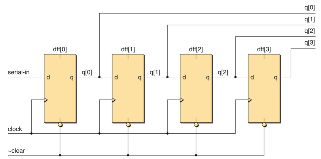
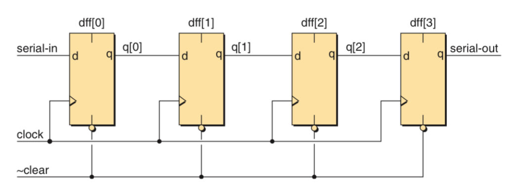
When the clear input is active, all the values are cleared to logic 0. When the first active edge occurs on the clock input, the serial in input is 1, so this value is loaded into the first flip-flop, at the same time, the 0 value from the first is loaded on to the second, and so on.
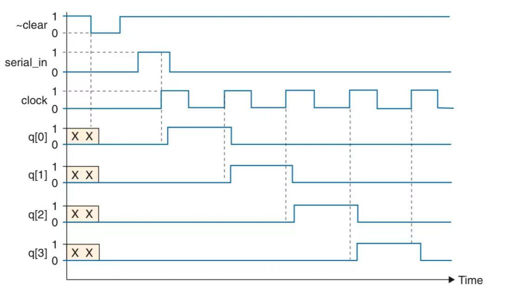
Each flip-flop exhibits a delay between seeing an active edge on the clock input and ensuing response on its q output. These delays provide sufficient time for the next flip-flop in the chain to load the value from the previous stage before that value changes.
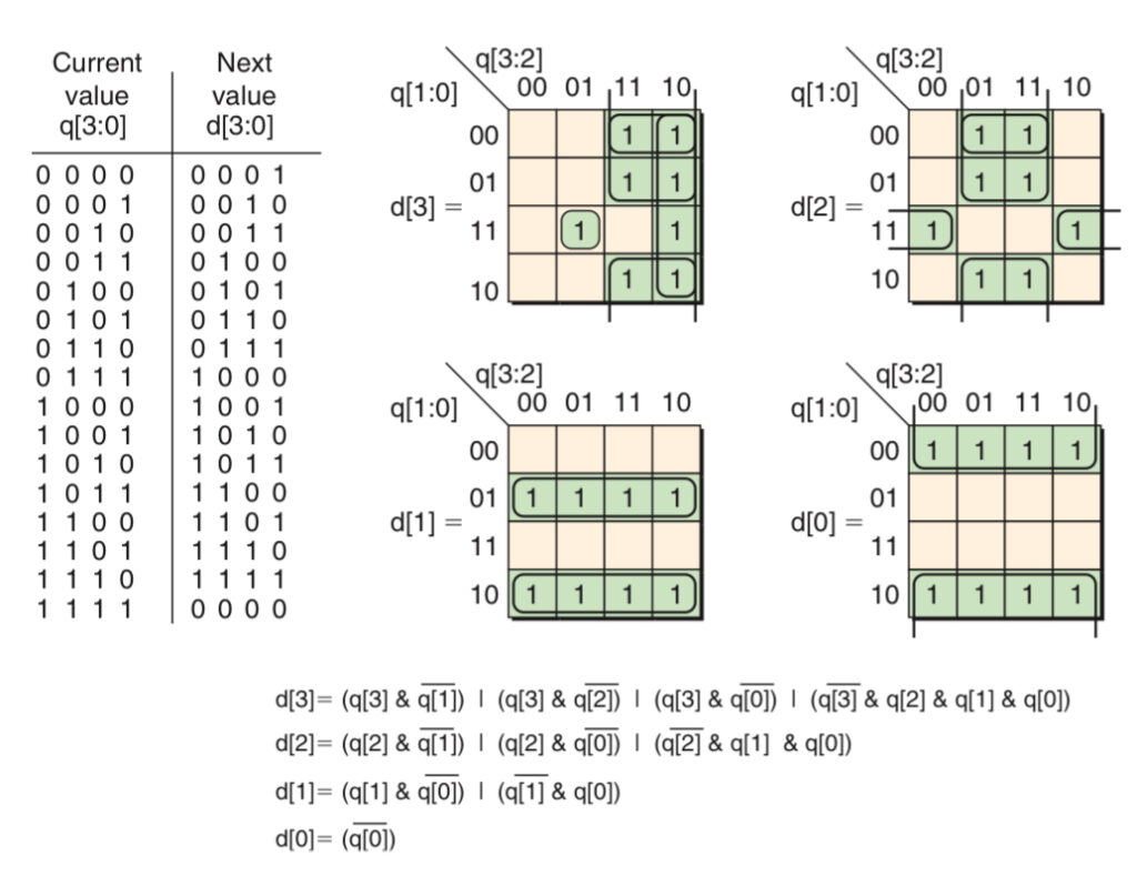
Counters
Counters are widely used in digital systems. The number of states that the counter will sequence through before returning to its original value is called the modulus of the counter. E.g. modulo-16 means that it can count 16 numbers from 0000 to 1111.
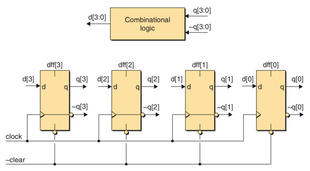
The four flip-flops are used to store the current count value that is displayed on their q[3:0] output. A block of combinational logic is needed to generate the next value d[3:0] which is based on the current value q[3:0].
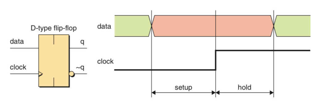
Setup & Hold Times
There are two parameters called the setup and hold times that describe the relationship between the flip-flop’s data and clock inputs. The value of the data input may be 0 or 1, it can change back and forth very quickly. However, it must settle one way or the other before the setup time and the value presented to the data input must remain stable for the hold time following the clock.