The Fabrication Process
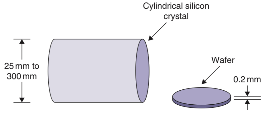
The construction of integrated circuits requires an environment that must be extremely clean, the impurities in material have to be so low as to be measured in parts per billion. The process begins with the growing of a crystal of pure silicon in the form of a cylinder, the cylinder is cut into slices called wafers.
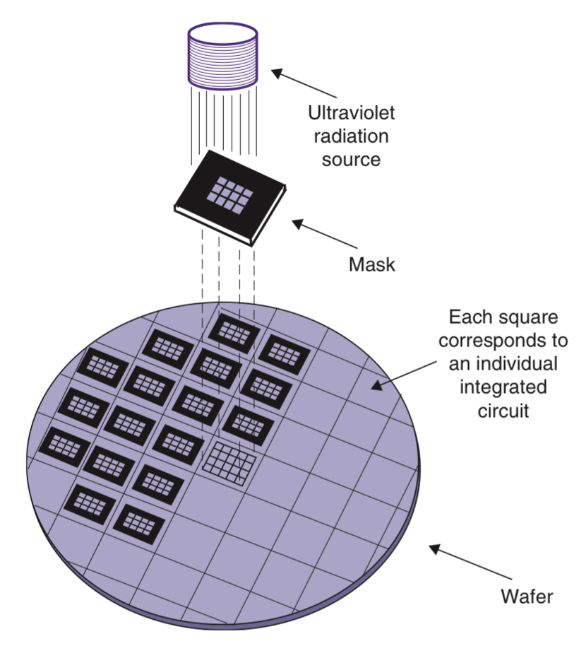
The most commonly used fabrication process is optical lithography, in which ultraviolet light is passed through a photo mask, and patterns are formed by areas that are either transparent or opaque to UV frequencies. Each Wafer contains hundreds or thousands of identical integrated circuits and the circuits are duplicated side by side on the wafer, this process is called a step-and-repeat process.
Fabrication Process in N-MOSFET
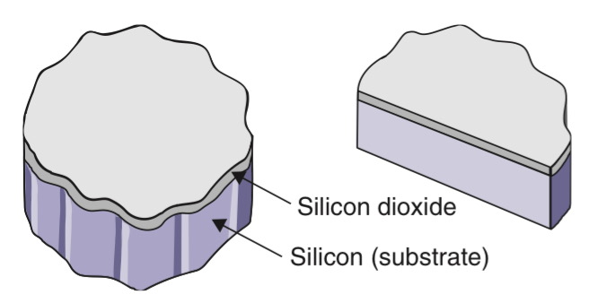
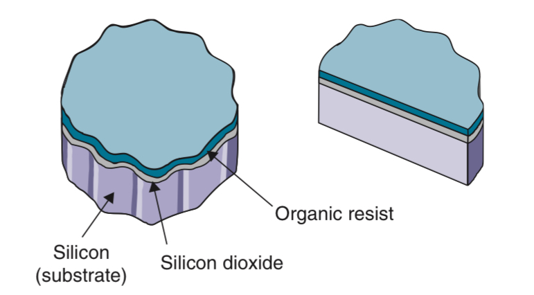
The wafer is referred to as the substrate, meaning the “base layer.” The first stage is to grow or deposit a thin layer of silicon dioxide across the entire surface of the wafer by exposing it to oxygen in a high-temperature oven.
The wafer is then coated with a thin layer of organic resist after it has cooled.
A mask is created and ultraviolet light is applied, the UZ light breaks down the molecular structure of the resist but doesn’t have any effect on the silicon dioxide or the pure silicon.
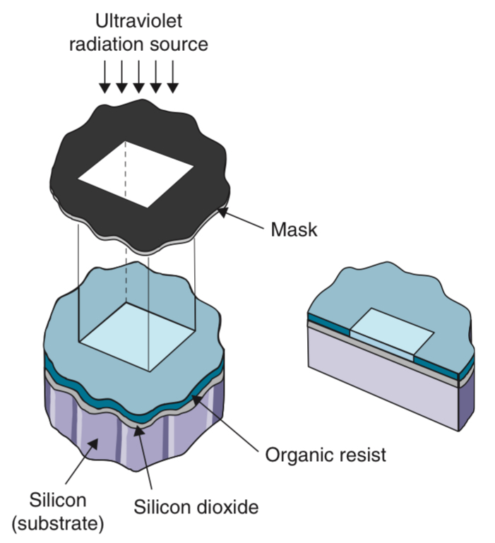
After the area under the mask has been exposed, the wafer is moved, and it is then bathed in an organic solvent to dissolve the degraded resist.
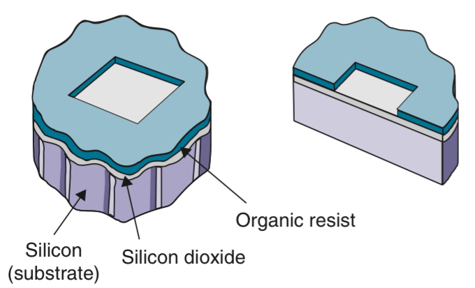
After that, the wafer undergoes a process known as etching, in which an appropriate solvent is used to dissolve any exposed silicon dioxide without having any effect on the organic resist or the pure silicon.
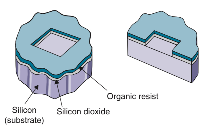
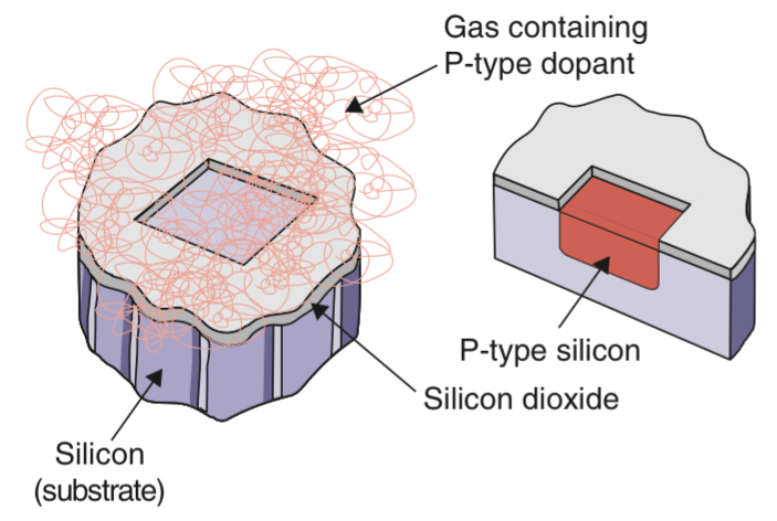
Next, the wafer is placed in a high-temperature oven where it is exposed to a gas containing the selected dopant. The atoms in the gas diffuse into the substrate, resulting in a region of doped silicon.
In the original MOS technologies, the gate electrode was metallic, however, in modern processes, the gate electrode is formed from polycrystalline silicon.
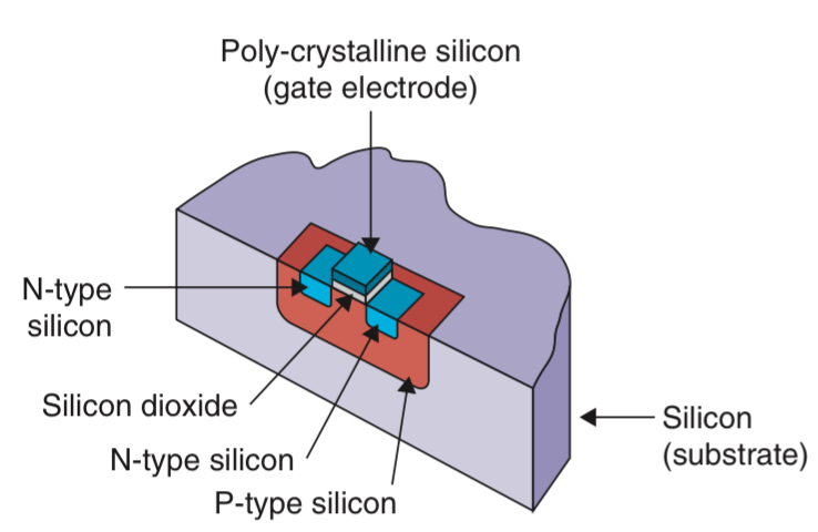
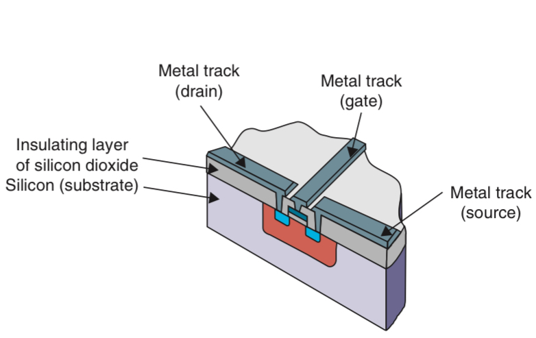
Another layer of insulating silicon dioxide is grown across the surface of the wafer. Holes are etched through the silicon dioxide in areas in which it is desired to make connections, and a metallization layer of interconnections called tracks is deposited. The tracks are used to connect groups of transistors to form primitive logic gates and to connect groups of these gates to form more complex functions.
The layers of silicon dioxide are also selectively etched with holes that are filled with conducting metal and are known as vias, these allow connections to be made between the various tracking layers.
Packaging Process
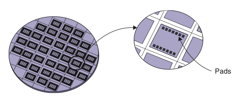
Areas of aluminium or copper called pads are constructed at the edges of each integrated circuits, some of the pads are used to supply power to the device, while the rest are used to provide input and output signals to the components in the chip.
Next is a step known as overglassing, the entire surface of the wafer is coated with a final barrier layer of silicon dioxide which provides physical protection for the underlying circuits from moisture and other contaminants.
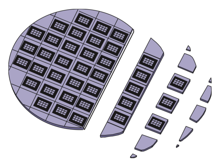
In wafer probing, the individual circuits are tested while they are still part of the wafer. An automated tester places probes on the device’s pads, provides corresponding inputs to the pads and monitors the corresponding signals returned from the output pads. The completed circuits is known as die, they are separated by marking the wafer with a diamond scribe and fracturing it along the scribed lines.
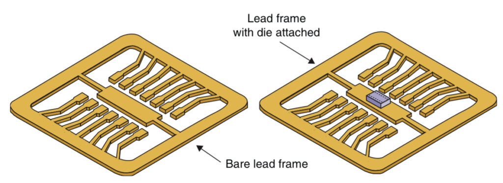
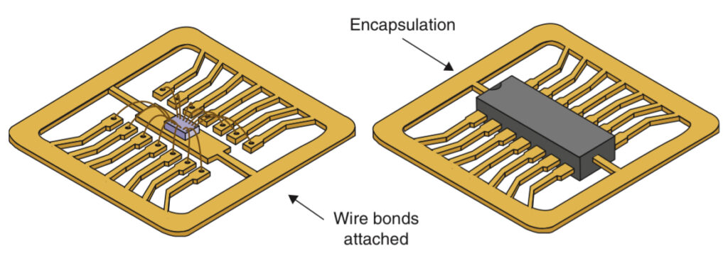
The die is then attached to a metallic lead frame using an adhesive. The adhesive is used to conduct heat away from the die when it is operating. An automatic wire-bonding tool connects the pads on the die to the leads on the frame. The whole assembly is then encapsulated in a block of plastic.
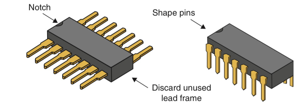
Notch is formed at one end of the package so that the users will know which end is which. A rectangular device with pins on two sides is called a Dual In-Line Package or a DIP. Other packages can be square and have pins on all four sides. These pins on the package that are intended to go all the way through the circuit board use a mounting technique called Lead Through Hole (LTH).
Different Types of IC
Transistors can be divided into a variety of flavors called families or technologies.
- Bipolar Junction Transistor (BJT). If BJTs are connected together in a certain way, the resulting logic gates are classed as Transistor Transistor Logic (TTL).
- An alternative method of connecting the same transistors results in logic gates classed as Emitter-Coupled Logic (ECL)
- Another family is MOSFETs.
Integrated circuits can also use a combination of technologies, e.g. BiCMOS Inverter
Moore’s Law
Moore stated the trend of a variety of electronics, including the number of transistors that can be constructed in a certain area of silicon doubles about every 18 months, the price per transistor halves above every 18 months, and the performance of microprocessors doubles about every 18 months.